Le58083
Data Sheet
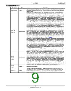
Signal Processing Channels (CHx)
These blocks do the transmission processing for the voice channels. Part of the processing is analog and is interfaced to the VIN
and VOUT pins. The remainder of the processing is digital and is interfaced to the Time Slot Assigner (TSA) block.
SLIC Device Interface (SLI)
This block communicates digitally with the SLIC device circuits. It sends control bits to the SLIC devices to control modes and to
operate LEDs and optocouplers. It also accepts supervision information from the SLIC devices and performs some filtering.
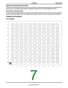
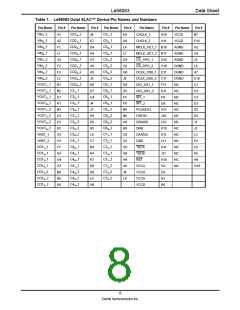
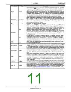
CONNECTION DIAGRAM
121-Pin BGA
VIN4_1
VOUT 4_1
NC
VIN4_2
VOUT 4_2
NC
C53_1
C43_1
C33_1
CD23_1
CD13_1
NC
C43_2
C33_2
CD23_2
CD13_2
C73_1
C63_1
NC
DGND
VCCD
C73_2
C63_2
C53_2
NC
C34_2
CD24_2
CD14_2
NC
C74_2
C64_2
C54_2
C44_2
INT_2
INT_1
C31_2
C41_2
C51_2
DRA/DD
DXB
DXA/DU
TSCB
NC
VCCA
AGND
AGND
VCCA
VIN3_2
VOUT 3_2
NC
C54_1
C44_1
L
K
DRB
FS/FSC
C34_1
J
H
VREF_2
VREF_1
VIN3_1
VOUT 3_1
NC
AGND
VCCA
VIN2_2
VOUT 2_2
NC
RST
TSCA
CD24_1
CD14_1
CD11_1
CD21_1
C31_1
PCLK/
DCL
C74_1
C64_1
C51_1
C61_1
C71_1
NC
G
F
DIO_1/
S1_1
VCCD
DGND
DCLK_1/
S0_1
CD12_1
CD22_1
C32_1
C32_2
C42_2
C52_2
E
D
C
B
A
CS_1/
PG_1
DIO_2/
S1_2
C62_1
C72_1
CS_2/
PG_2
DCLK_2/
S0_2
NC
NC
NC
C41_1
MCLK_1/
E1_1
MCLK_2/
E1_2
VOUT 1_1
VOUT 2_1
C42_1
C52_1
CD12_2
CD22_2
C62_2
C72_2
CD11_2
CD21_2
C61_2
C71_2
VOUT 1_2
VCCD
DGND
VIN1_1
VIN2_1
CHCLK_1
CHCLK_2
VIN1_2
1
2
3
4
5
6
7
8
9
10
11
7
Zarlink Semiconductor Inc.

 ZARLINK [ ZARLINK SEMICONDUCTOR INC ]