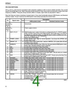
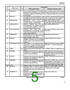
GP2021
TIC is an internal signal with a default period of 99999·90µs.
It is used to latch measurement data (Epoch count, Code
phase, Code DCO phase, Carrier DCO phase and Carrier
cycle count) of all 12 channels at the same instant. Its
period can subsequently be changed, by writing to the
PROG_TIC_HIGH and PROG_TIC_LOW registers, or
toggling the FRONT_END_MODE bit of the
SYSTEM_SETUP register.
the front end by SAMPCLK. This data is then input to the
GP2021 as 2-bit data on either the SIGN0, MAG0, or
SIGN1, MAG1 inputs, where it is re-sampled at the next
rising edge of SAMPCLK. These signals are then
distributed to the 12 tracking modules.
When a GP2015 or GP2010 front end is used, the data
represents a band-limited signal at an IF centered on
4·309MHz. Sampling at 5·714MHz aliases it to an IF of
1·405MHz.
MEAS_INT is a signal derived from theTIC counter. It may
be used by the microprocessor as a software module
switching interrupt either by using the MEAS_INT output
or by reading the ACCUM_STATUS_B or
MEAS_STATUS_A register. MEAS_INT is activated at
each TIC and 50ms before each TIC so long as the TIC
period is greater than 50ms. If the TIC period is less than
50ms, MEAS_INTis activated only at each TIC. It is cleared
by reading either the ACCUM_STATUS_B or
MEAS_STATUS_A register, depending upon the
MEAS_INT_SOURCE bit of the SYSTEM_SETUP
register.
In Complex_lnput mode, the down converted satellite signal
is applied direct to the GP2021 at its SIGN0, MAG0, SIGN1
and MAG1 inputs, which act as In-Phase Sign, In-Phase
Magnitude, Quadrature Sign and Quadrature Magnitude
respectively. These signals are sampled at 5·833MHz
within the correlator and then passed to the tracking
modules.
Address Decoder
The Address Decoder performs address decoding for the
correlator.
TIMEMARK is also derived from TIC and may be output
on one of the discrete output pins. This signal is intended
to be used as an accurate 1 pulse per second timing
reference, aligned to UTC (Co-ordinated Universal Time),
with a pulse width of 1ms. A true 1pps output needs
extensive software algorithms to be produced; without this
the TIMEMARK will not be aligned to UTC.
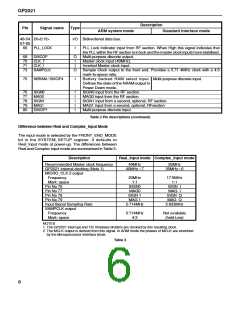
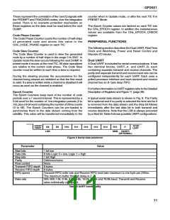
Bus Interface
The Bus Interface controls the transfer of data between
the external 16-bit wide data bus and the internal 32-bit
data bus.
Apart from the code and carrier DCO increment values,
all data transfers are 16 bits wide. Write operations to the
code and carrier DCOs are 32- bit data transfers, in which
the high 16-bit word must be written immediately before
the low 16-bit word. Note that the write cycle to write cycle
delay of 300ns referred to in the Microprocessor Interface
does not apply between the first and second write cycles
for 32-bit DCO data transfers. For further information see
the Microprocessor Interface section, page 15
TIMEMARK has two methods of operation but in both
cases TIMEMARK rising edges are generated coincident
with the rising edges of TIC. Therefore, for TIMEMARK to
be aligned with UTC, TIC must be aligned with UTC. This
is done by modifying the TIC period for a single TIC cycle,
then setting it back to its original value, thus slewing the
phase of TIC. TIMEMARK may be generated by setting
the TIMEMARK_ARM bit in the TIMEMARK_CONTROL
register, in which case the next TIC will generate a rising
edge at TIMEMARK and clear the TIMEMARK_ARM bit.
Alternatively TIMEMARK may be generated as a
programmable integer number of TlCs, again under the
control of the TIMEMARK_CONTROL register.
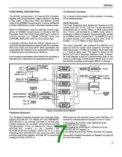
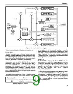
Tracking Modules
The Tracking Modules are 12 identical signal tracking
channels numbered CH0 to CH11, each with the block
diagram shown in Figure 5. These blocks generate the
data used to track the satellite signals. There is no overwrite
protection mechanism on this data. For further information
see the section on Controlling the GP2021, page 24
Status Registers
There are four status registers (ACCUM_STATUS_A, _B,
_C and MEAS_STATUS_A). These contain flags
associated with the accumulated and measurement data
held on each of the 12 channels. Some system level status
bits also appear in these registers.
Each Tracking Channel can be individually programmed
to operate in either Update or Preset mode. Update mode
is the normal mode of operation. Preset mode is a special
mode of operation where writes to certain registers are
delayed until the next TIC to allow synchronisation of
registers and presetting of the code DCO phase. For further
information see the Preset Mode section in the Detailed
Operation of the GP2021, page 28.
Sample Latches
The Sample Latches synchronise data from the front end
to the internal SAMPCLK. In Real_lnput mode the down
converted satellite signal can be sampled at the output of
8

 ZARLINK [ ZARLINK SEMICONDUCTOR INC ]