GP2021
Reset
XIN
XOUT
It is possible for the software to reset either UART
independently via the RESET_CHx registers. A hardware
reset affects both UARTs. During a UART reset, the
contents of all Control and Status registers will be cleared.
In addition the Transmit and Receive FlFO’s will be emptied
and the TX outputs will be held low.
680k
10M
22p
22p
32·768kHz
CRYSTAL
Channel Loopback
V
SS
V
SS
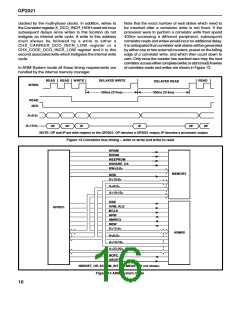
For system test purposes, a loopback facility is provided
for each channel, controlled by the Configuration registers.
In loopback, the TX output is set high.
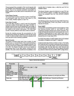
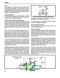
Figure 7 Recommended crystal oscillator circuit
Watchdog Reset registers respectively. In addition, the
watchdog is reset during a System Reset.
Real Time Clock (RTC) and Watchdog
This block consists of a 32·768kHz crystal oscillator, a fixed
divider, a 24-bit counter, a Watchdog function and three
8-bit data registers. XIN and XOUT are the crystal in and
crystal out connections to the oscillator circuit. A recom-
mended crystal oscillator circuit is shown in Fig. 7. When
the Real Time Clock is not being used, XIN must be tied
low.
For further information on the registers refer to the Detailed
Description of Registers (page 28).
Power and Reset Control
This block performs two functions: Power Control and
System Reset Generation
Power Down Mode
The first divider is a fixed divide-by-32768 giving a 1Hz
output. The counter then counts seconds, giving a
maximum time of 194 days. The time is output in three
8-bit registers with the data being latched when a read is
performed to the LS register (the register holding the least
significant byte of the clock data). On reaching its maximum
count, the count is frozen (i.e. all ones), until being reset.
In order to allow power conservation within a battery backup
system, the GP2021 provides a Power Down mode, in
which the supply voltage may drop to a minimum of 2·2V,
thereby minimising the supply current. In this mode all
functions within the GP2021 are disabled except for the
Real Time Clock.
The GP2021 is placed in Power Down mode by taking the
POWER_GOOD pin Low. In ARM System mode with the
NBRAM pin held low, the initiation of Power Down mode
is delayed until just after a falling edge of MICRO_CLK so
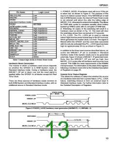
as not to corrupt battery backed RAM. Fig. 8 shows a
suggested circuit implementation. Table 7 shows output
logic levels in Power Down mode.
In Power Down mode the Real Time Clock continues to
run, but the data registers cannot be accessed. When
normal power is restored, the software can determine the
elapsed time whilst in Power Down mode, thereby assisting
in estimating the current position of GPS satellites and so
reducing Time-To-First-Fix.
TheWatchdog generates a System Reset (see Powerand
Reset Control) if the Watchdog Reset address has not
been written to for a period of approximately 2 seconds.
The watchdog function is inhibited whilst in Power Down
mode and can be disabled via a bit in the System
Configuration register.The software is able to reset the Real
Time Clock and Watchdog via the Clock Reset and
In Power Down mode all inputs and l/Os except
POWER_GOOD and XIN are internally switched to known
logic levels to prevent extraneous switching from causing
excessive power consumption, and may therefore be left
floating. All the l/O pins (D<15:0>, MULTI_FN_IO and
DISCIO) have their output drivers driven to the high
impedance state.
D1
BATTERY SUPPLY
V
DD
15V SUPPLY
T1
R1
C2
GP2021
T2
VOLTAGE
SENSOR
C1
R2
POWER_GOOD
V
SS
V
SS
Figure 8 Suggested battery back up configuration
12

 ZARLINK [ ZARLINK SEMICONDUCTOR INC ]