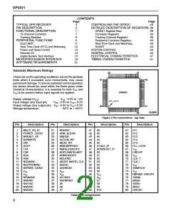
GP2021
Description
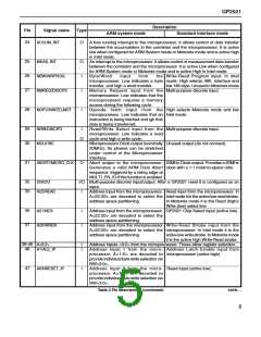
Pin
Signal name
Type
I/O Bidirectional data bus.
ARM system mode
Standard interface mode
48-54
57-65
66
D0<0:15>
PLL_LOCK
I
PLL Lock Indicator input from RF section. When High this signal indicates that
the PLL within the RF section is in lock and the master clock inputs have stabilised.
Multi-purpose discrete output.
68
70
71
73
DISCOP
CLK_T
CLK_I
O
I
Master clock input (40MHz).
I
Inverted Master clock input.
SAMPCLK
O
Sample Clock output to the front end. Provides a 5.71 4MHz clock with a 4:3
mark-to-space ratio.
75
NBRAM / DISCIP4
I
Battery backed RAM select input. Multi-purpose discrete input.
Defines the state of the NRAM output in
Power Down mode.
SIGN0 input from the RF section.
MAG0 input from the RF section.
SIGN1 input from a second, optional, RF section.
MAG1 input from a second, optional, RFsection
Multi-purpose discrete input.
76
77
78
79
80
SIGN0
MAG0
SIGN1
MAG1
DISCIP1
I
I
I
I
I
Table 2 Pin descriptions (continued)
Difference between Real and Complex_lnput Mode
The input mode is selected by the FRONT_END_MODE
bit in the SYSTEM_SETUP register. It defaults to
Real_lnput mode at power-up. The differences between
Real and Complex input mode are summarised in Table 3.
Description
Real_lnput mode Complex_lnput mode
Recommended Master clock frequency
GP2021 internal clocking (Note 1)
MICRO_CLK 2 output
Frequency
40MHz
40MHz47
35MHz
35MHz46
20MHz
1:1
17·5MHz
1:1
Mark: space
Pin No 76
Pin No 77
Pin No 78
Pin No 79
Input Signal Sampling Rate
SAMPCLK output
Frequency
SIGN0
MAG0
SIGN 1
MAG 1
5·714MHz
SIGN_I
MAG_I
SIGN_Q
MAG_Q
5·833MHz
5·714MHz
4:3
Not available
(held Low)
Mark: space
NOTES
1. The GP2021 interrupt and TIC timebase dividers are clocked by this resulting clock.
2. The MCLK output is derived from this signal. In ARM mode the phases of MCLK are stretched
by the Microprocessor Interface block.
Table 3
6

 ZARLINK [ ZARLINK SEMICONDUCTOR INC ]