GP2021
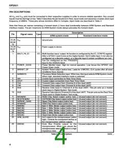
PIN DESCRIPTIONS
All VSS and VDD pins must be connected to their respective supplies in order to ensure reliable operation. Any unused
inputs must be tied high or low. Table 2 describes the pin functions in Real_lnput mode and assumes a master clock input
frequency of 40MHz. Those pins whose functions differ in Complex_lnput mode are described in Table 3.
Note that those pin names containing a forward slash (/) have dual functionality between ARM System and Standard
Interface modes. The pin mnemonic for ARM System mode always precedes the forward slash.
Description
Pin
Signal name
Type
ARM system mode
Ground pins
Standard interface mode
15,35
56,69
72
VSS
2
14,34
55,67
74
VDD
1
Power supply to device
1
MULTI_FN_IO
I/O Multi-function input / output. Its function is configured by the IO_CONFIG register.
After a GP2021 reset it acts as the Digital System Test Enable input. It can also be
configured as a discrete output, or a discrete input if certain conditions are met.
Can be configured as the TRIGGER
input to the DEBUG block
Power Monitor input. High for normal operation. Low forces the GP2021 into
Power Down mode.
System Reset output (active low). Lasts for 4 MICRO_CLK cycles after all reset
conditions have cleared.
Processor Mode Selection input. When low, this input selectsARM System mode.
When high, standard Interface mode is selected.
2
3
4
POWER _GOOD
NRESET_OP
NARMSYS
I
O
I
5
6
7
8
9
XIN
I
Crystal input connection to Real Time Clock.
Crystal output connection from Real Time Clock.
Transmit Data output from Channel A of the dual UART.
Transmit Data output from Channel B of the dual UART.
Receive Data input to Channel A of the dual UART. This pin acts as a master
clock input in Digital System Test mode.
XOUT
TXA
TXB
RXA
O
O
O
I
10
RXB
I
Receive Data input to Channel B of the dual UART. This pin acts as the RealTime
Clock reset in Digital System Test mode.
11
12
13
16
17
18
19
20
21
22
NROM/NC
NEEPROM/NC
NSPARE_CS/NC
NRAM/NC
NW0/NC
NW1/NC
NW2/NC
NW3/NC
NRD/NC
O
O
O
O
O
O
O
O
O
O
ROM Chip Select output (active low). Unused output (do not connect)
EEPROM Chip Select output (active low) Unused output (do not connect).
Spare Chip Select output (active low).
RAM Chip Select output (active low).
Unused output (do not connect).
Unused output (do not connect).
Byte 0 Write Strobe output (active low). Unused output (do not connect.)
Byte 1 Write Strobe output (active low). Unused output (do not connect).
Byte 2 Write Strobe output (active low). Unused output (do not connect).
Byte 3 Write Strobe output (active low). Unused output (do not connect).
Read Data Strobe output (active low).
Unused output (do not connect).
ARM_ALE/NC
ALE output to the microprocessor (active Unused output (do not connect).
high). Controls the transparent latches at
the microprocessor address outputs.
Data Bus Enable output to the Unused output (do not connect).
microprocessor. When Low, places the
23
DBE/NC
O
microprocessor data bus drivers in a high
impedance state.
Table 2 Pin descriptions
cont…
4

 ZARLINK [ ZARLINK SEMICONDUCTOR INC ]