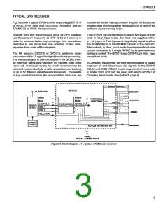
GP2021
FUNCTIONAL DESCRIPTION
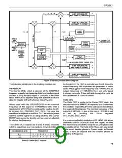
12-Channel Correlator
The GP2021 incorporates a 12-Channel GPS Correlator,
together with microprocessor support functions including
a Dual UART, a Real Time Clock and Memory Control
Logic for theARM60 microprocessor. It can be configured
for eitherARM System mode or Standard Interface mode.
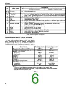
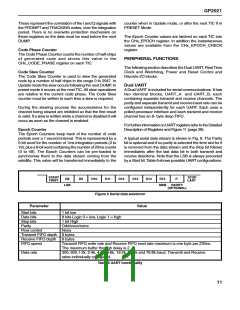
Fig. 4 shows a block diagram of the correlator. It consists
of the following blocks:
Clock Generator
The Clock Generator block divides the frequency of the
master clock CLK_T/CLK_I by 6 or 7 to give the internal
multi-phase set of clocks. When in Real_lnput mode
CLK_T/CLK_I will normally be a 40MHz clock, which is
divided by 7. When in Complex_lnput mode it will normally
be at 35MHz which is divided by 6. The SAMPCLK pin is
an output giving a 4:3 mark-to-space ratio clock at
40 MHz 47 (= 5·714MHz) in Real_lnput Mode.
When in ARM System mode the Memory Control Logic
allows an ARM60 microprocessor to interface with the
Correlator, Real Time Clock, Dual UART and a variety of
memory devices (i.e. SRAM, EPROM, Flash and
EEPROM), without the need for external glue logic.
In Standard Interface mode the GP2021 allows most 16-
and 32-bit microprocessors to interface with the Correlator,
Real Time Clock and Dual UART. More specifically, this
mode allows the interface to be configured for either Intel
or Motorola style microprocessor interfaces.
The Clock Generator also produces the MICRO_CLK
signal at half the master clock frequency (20 MHz for
Real_lnput mode, 17·5 MHz for Complex_lnput mode) with
a 1:1 mark-to-space ratio. This signal is output on the
MICRO_CLK pin in Standard Interface mode. However,
its main purpose is that of a synchronising clock to the
memory control logic in ARM System Mode and it is from
this that the processor clock output, MCLK, is derived.
In the functional description which follows the correlator is
described first, followed by the peripheral functions.
MULTIPHASE
CLOCKS
TRACKING
MODULE
CLK_T
CLK_I
CLOCK
REGISTER
SELECTS
ADDRESS
DECODER
A<9:2>
GENERATOR
CHANNEL 0
SAMPCLK
MICRO_CLK
TRACKING
MODULE
32-BIT BUS
D<15:0>
BUS
CHANNEL 1
INTERFACE
CONTROL
MEAS_INT
TIC
TIMEBASE
GENERATOR
ACCUM_INT
TRACKING
MODULE
CHANNEL 2
STATUS
REGISTERS
INTERNAL
SAMPCLK
TRACKING
MODULE
LATCHED
SIGN0 AND MAG0
SYSTEM
STATUS
BITS
CHANNEL 3
SIGN0 AND MAG0
SIGN1 AND MAG1
G
G
G
G
G
G
SAMPLE
LATCH
LATCHED
SIGN1 AND MAG1
V
DD
POWER
SUPPLY
V
TRACKING
MODULE
SS
CHANNEL 11
Figure 4 Correlator block diagram
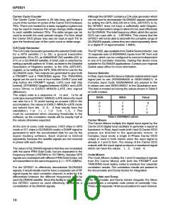
Timebase Generator
The Timebase Generator produces four important timing
signals: ACCUM_INT, TIC, MEAS_INT and TIMEMARK.
ACCUM_INT is an interrupt provided to control data
transfer between the correlator accumulators and the
microprocessor. It may be detected by means of the
After power-up this interrupt occurs every 505·05µs. Its
period can subsequently be changed in one of 3 ways:
1. By toggling the FRONT_END_MODE bit of the
SYSTEM_SETUP register,
2. By toggling the INTERRUPT_PERIOD bit of the
SYSTEM_SETUP register, or
ACCUM_INT
output
or
by
reading
the
ACCUM_STATUS_A register (where bit 15 is a flag
indicating that ACCUM_INT has occurred since the
previous read of this register). ACCUM_INT is cleared by
reading ACCUM_STATUS_A.
3. By writing directly to the PROG_ACCUM_INT register.
See section Detailed Description of Registers on page 28
for more information.
7

 ZARLINK [ ZARLINK SEMICONDUCTOR INC ]