GP2021
required frequency by programming the Code DCO even
though the code output is disabled. A typical value is the
frequency for the nominal code chipping rate, so that the
SIGN and MAG counts are over a millisecond.
TEST_SOURCE: When high this bit enables a self-test
generator formed from the CH0 Code Generator.The data
replaces the SIGN0 and MAG0 inputs. It has a chip rate
and phase set by the CH0_CODE_DCO and a carrier
frequency set by the CH0_CARRIER_DCO. The code is
set by writing the appropriate start value into the
CH0_SATCNTL register, and the CH0_SLEW_COUNTER
can be programmed to delay the start of the code
generation by a number of half code chips.
The results of monitoring the front end of the receiver may
be used for fault diagnosis and also for tuning the
parameters in the software for optimum satellite tracking
with the particular front end or SIGN/MAG duty cycle.
To find the duty cycle of the SIGN signal, channel 5 is
used. The In-phase accumulator CH5_I_PROMPTwill add
11 for each SIGN sample at high and will add 21 for each
SIGN sample at low, so if the duty cycle is correct at 50%,
the sum will always be close to zero and only differ by the
imbalance of sampling at the beginning and end of the
integration period.
The three most significant bits of the Carrier DCO are
decoded to give the SIGN with 50% of highs and the MAG
with 25% of highs. The sign of the data pattern is set by
TEST_DATA, EXORed with the CH0 C/A code.
TEST_DATA: This bit sets the sign of the modulation of
the test data generated when TEST_SOURCE is set.
The duty cycle may be calculated as follows:
TEST_CACODES: When high, the inverted PROMPT
codes for all channels, 0 to 11, are available for output on
data bus bits 0 to 11 and can be seen in parallel by a read
to any CH6 to CH11 read address.
N = Total no. of samples in integration period
NSIGN1 = Total no. of samples for which SIGN was high
NSIGN0 = Total no. of samples for which SIGN was low
EN_SCANPATH: When high the chip is in scan test mode,
whereby:
ACC5 = Total value in the CH5_1_PROMPT accumulator,
as read after a DUMP.
N = NSIGN11NSIGN0
DISCIP 1
becomes
becomes
becomes
SCAN_IN
ACC5 = NSIGN12NSIGN0
DISCOP
SCAN_OUT
SCANCLK
SCANSEL
SIGN duty cycle = R s = NSIGN1/N = (N1ACC5)/2N
(nominally 50%)
MULTI_FN_IO
NOPC/NINTELMOT becomes
To find the duty cycle of the MAG signal, channel 11 is
used. The In-phase accumulator CH11_I_PROMPT will
add 23 for each MAG sample at high and will add 21 for
each MAG sample at low. If the duty cycle is correct (30%),
the sum will be 21·63(Number of samples) plus an
allowance for the imbalance of sampling at the beginning
and end of the integration period. The duty cycle may be
calculated as follows:
It should be noted that the DISCOP = SCAN_OUT function
may be over-ridden by the DlSCOP_SELECT_100KHZ
function of SYSTEM_SETUP. It should also be noted that
for correct operation the MULTI_FN_IO pin should be
configured as a Discrete or Scan Clock Input via the
IO_CONFIG register.
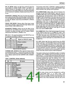
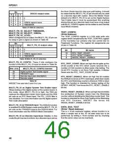
PATH_SEL<2:0>: To allow for simple factory testing of
the chip, the GP2021 contains six separate scan paths,
one for each of the major counters in the chip. Only one of
these paths may be enabled at any time and the scan
path to be used is selected via the PATH_SEL <2:0> bits
as shown in Table 28.
N = Total No of samples in integration period
NMAG3 =Total number of samples for which MAG was high
NMAG1 = Total number of samples for which MAG was low
ACC11 = Total value in the CH11_I_PROMPT accumulator,
as read after a DUMP.
N = NMAG31NMAG1
PATH_SEL
Scan path selected
<2:0>
ACC11 = 233(NMAG3)2NMAG1
MAG duty cycle, Rm = NMAG3/N = 2(N1ACC11)/2N
(nominally 30%).
000
001
010
011
100
101
11X
RTC counters
ACCUM_INT counter
TIC counter
100kHz output counter
Timemark pulse width counter
PLL_LOCK filter counter
Not used
TM_TEST: When High this bit puts all theTracking Modules
into a test mode, where it is possible to write to all
CHx_CARRIER_CYCLE_COUNTERs
CHx_CODE_PHASE_COUNTERs.
and
all
Table 28
42

 ZARLINK [ ZARLINK SEMICONDUCTOR INC ]