GP2021
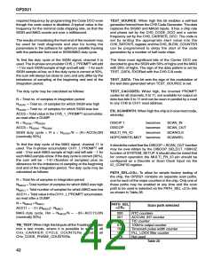
Bit 8: Set during a system reset, when the source of the
input in Standard Interface mode. Similarly, NMREQ could
be used as a discrete input in Standard Interface mode
but not in ARM System mode.
reset is a PLL_LOCK failure.
Bit 9: Set during a system reset, when the source of the
reset is the Watchdog.
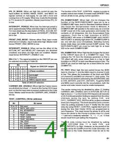
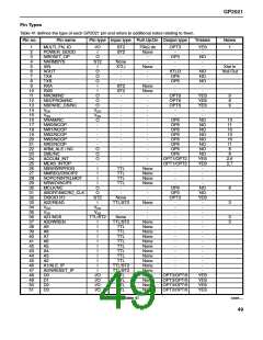
Bit
Input pin
RXB
RXA
DISCOP
DISCIP
MAG1
SIGN1
MAG0
SIGN0
15
14
13
12
11
10
9
Bit 10: Set during a system reset, when the source of the
reset is a POWER_GOOD failure.
Bit 11: Set during a system reset, when the source of the
reset is the external NRESET_IP. Note that
this reset source is only available in Standard
Interface mode.
8
MULTI_FN_IO
NBRAM
DISCIO
NARMSYS
NBW/WRPROG
NMREQ
7
6
5
4
3
2
1
0
CHIP_REVISION
(Read Addresses)
The CHIP_REVISION register is a read only register
which exists as the high 4 data bits of the Wait state, System
Configuration and System Error Status registers. A read
of any of these three registers will output the
CHIP_REVISION information on bits 15 to 12. This register
is intended to allow software discrimination of revisions of
the GP2021, both pre-production revisions and possible
customer-specific variants. The initial production version
of the GP2021 will have a CHIP_REVISION of 0011.
NOPC/NINTELMOT
NRW
Table 35
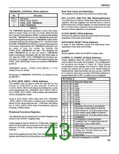
IO_CONFIG Write: The IO_CONFIG write location allows
the configuration of the multi-purpose I/O pins DISCIO and
MULTI_FN_IO.The register bit assignments are as shown
in Table 36
DATA_RETENT
(Write/Read Address)
This is a byte wide Read/Write register which can be used
to store a predetermined value, which can be interrogated
in order to determine whether a total power loss (below
the data retention level ) has occurred.
Bit
Bit name
15 to 13 Not Used
12
11
10
9 to 8
7 to 4
3
2
1
0
MULTI_FN_IO_SELECT_TIMEMARK
MULTI_FN_IO_SELECT_1 00KHZ
MULTI_FN_IO_LEVEL
MULTI_FN_IO_CONFIG
Not Used
DISCIO_SELECT_TIMEMARK
DISCIO_SELECT_1 00KHZ
DISCIO_LEVEL
GENERAL CONTROL
IO_CONFIG
(Write/Read Address)
The IO_CONFIG register is a full 16-bit wide read/write
register containing two separate elements: a 16-bit wide
read location which allows the controlling microprocessor
to view the input level on all the Discrete and Multi Function
inputs, and a 16-bit wide write location for configuration of
the Discrete and Multi Function l/O pins.
DISCIO_CONFIG
Table 36
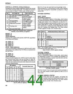
DISCIO_CONFIG: When set high this bit configures the
DISCIO pin as a discrete output, when low the DISCIO
pin is configured as a discrete input. NRESET low sets
the DISCIO_CONFIG bit low.
IO_CONFIG Read: A read of the IO_CONFIG address
will latch the logic level of a number of input pins and output
these levels to the microprocessor via the 16-bit data bus.
This allows the microprocessor to read the input levels on
all the discrete and multi-function Inputs from a single
location. The bit allocations are as sown in Table 35.
DISCIO_SELECT TIMEMARK,
DISCIO_SELECT_100KHZ,
DISCIO_LEVEL
When configured as an output, the DISCIO pin can be set
up to give a signal as determined by Table 37.
It should be noted that the usefulness of a number of these
inputs as discrete Inputs for System Control is dependent
upon the Interface Mode of the GP2021. For instance, it is
possible to use the NOPC/NINTELMOT pin as a discrete
input in ARM System mode if the DEBUG function is
disabled, whereas this pin could not be used as a discrete
At power on reset, the DISCIO output value = 0 setting is
chosen. The 100kHz square wave is derived from the
Master Clock and is useful for measuring its drift.
45

 ZARLINK [ ZARLINK SEMICONDUCTOR INC ]