GP2021
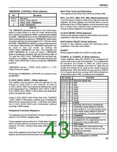
TIMEMARK_CONTROL (Write address)
Real Time Clock and Watchdog
The registers in the Real Time Clock are all byte wide.
Bit
Bit name
RTC_LS, RTC_2ND, RTC_MS, (Read Addresses)
The clock time is output in these three eight-bit read only
registers. All three registers are latched when a read is
performed of the LS Byte Register, so this should be read
first. In Power Down mode the clock continues to run but
access to these registers is not possible.
15 to 7
6 to 2
Not used
FREE_RUN_RATIO
FREE_RUN_TIMEMARK
ARM_TIMEMARK
1
0
Table 29
The TIMEMARK generator operates in one of two ways,
either in armed mode or in free run mode. (Note that the
term ‘armed’is not related toARM). In armed mode setting
theARM_TIMEMARK bit arms theTIMEMARK generator
which subsequently produces a TIMEMARK output pulse
coincident with the next rising edge ofTIC. This then resets
theARM_TIMEMARK bit ready for a new arming sequence
in the future. Alternatively, the TIMEMARK generator can
be used in free run mode, by setting the
FREE_RUN_TIMEMARK bit high. This disables the
ARM_TIMEMARK bit. In free run mode a TIMEMARK
pulse is produced coincident with the first rising edge of
TIC after the FREE_RUN_TIMEMARK bit has been set,
and then on an integer number of TlCs determined by the
FREE_RUN_RATIO bits. In free run mode the TIMEMARK
period is:
CLOCK RESET (Write Address)
Awrite to this address resets the clock divider and counter,
regardless of the data word written.
WATCHDOG RESET (Write Address)
A write to this address resets the watchdog timer,
regardless of the data word written.
DUART
All the registers within the DUART are byte wide.
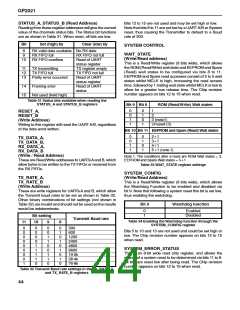
CONFIG_A, CONFIG_B (Write Address)
These registers allow the UARTs to be configured for
receive baud rate, parity and loopback. The configuration
bit functions are shown in Table 30. Other binary
combinations of bit settings (not shown in Table 30) are
invalid and should not be used as the results would be
indeterminate. Note that all bits are set Low by a UARTA/
B or a System reset, thus causing UARTA/B to default to a
receive baud rate of 300, no parity and no loopback.
TIMEMARK period = (FREE_RUN_RATIO11 )3TIC
Period (Free run mode)
All the bits of TIMEMARK_CONTROL are cleared to low
by NRESET.
Bit setting
11 10 9
Function
Receiver Baud rate
X_DCO_INCR_HIGH1 : (Write Address)
8
This register may be used to write the high bits for any
Carrier or Code DCO in any channel. A write to
X_DCO_INCR_HIGH must always be followed by a write
to the appropriate CHx_CARRIER_DCO_INCR_LOW or
CHx_CODE_DCO_INCR_LOW to define the destination
and to complete the action.
300
600
1200
2400
4800
9600
19.2k
38.4k
0
0
0
0
0
0
0
0
1
0
0
0
0
1
1
1
1
0
0 0
0 1
1 0
1 1
0 0
0 1
1 0
1 1
0 0
Using X_DCO_INCR_HIGH rather than CHx_CARRIER
_DCO_I NCR_H IGH gives a quicker way of loading the
whole DCOs values because the _LOW write may follow
the X_DCO_INCR HIGH write immediately (without
incurring a 300ns delay)
76.8k
Parity
13 12
0
1
No parity: bit not set or checked for
Odd parity: parity added so that the
total number of ‘1’s in the word is even
Even parity: parity added so that the
total number of ‘1’s in the word is even
Loopback
No loopback: normal operation
Loopback: the Tx output drives the Rx
input and Tx pin is held HIGH
Test mode
0
1
Peripheral Functions Registers
1
0
The addresses for the Peripheral Functions Registers are
shown in the GP2021 Register Map.
14
0
1
These registers may be either 8 or 16 bits wide. Registers
which are byte wide are accessed via the top 8 bits of the
data bus, D<15:8>. During a byte wide read D<7:0> are
held low.
15
0
Test mode bit in ChA used for chip
testing only. This bit must be set Low
for Normal operation
Test mode
Each of the registers for the Real Time Clock, Dual UART,
System and General Control functions are described below.
1
Table 30 Configuration of UARTs
43

 ZARLINK [ ZARLINK SEMICONDUCTOR INC ]