GP2021
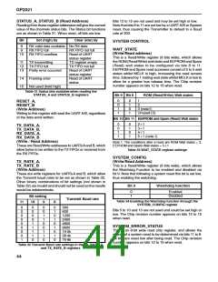
STATUS_A, STATUS_B (Read Address)
Bits 12 to 15 are not used and may be set high or low.
Note that bits 8 to 11 are set low by a UARTA/B or System
reset, thus causing the Transmitter to default to a Baud
rate of 300.
Reading from these register addresses will give the current
value of the channels status bits. The Status bit functions
are as shown in Table 31. When reset, all bits are low.
Bit
Set (high) by
RX valid data available No RX data
RX FIFO full RX FIFO not full
Clear (low) by
SYSTEM CONTROL
8
9
WAIT_STATE
(Write/Read address)
10 RX FIFO overflow
Read of UART
status register
TX register empty
TX FIFO not full
Read of UART
status register
Read of UART
status
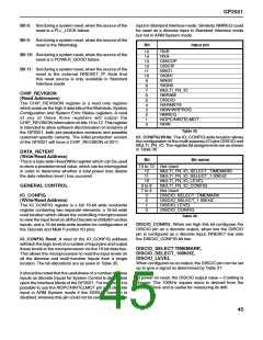
This is a Read/Write register (8 bits wide), which allows
the ROM (Read/Write) wait state and EEPROM and Spare
(Read) wait states to be configured via bits 8 to 11.
EEPROM and Spare read accesses consist of 2 to 5 wait
states whilst MCLK is high, increasing the read access
time, followed by 1 trailing wait state whilst MCLK is low to
allow for a greater bus release time. The Chip revision
number appears on bits 12 to 15 when read.
11 TX transmitting
12 TX FIFO full
13 Parity error occurred
14 Framing error
15 Not used (held high)
Table 31 Status bits available when reading the
STATUS_A and STATUS_B registers
Bit 9 Bit 8
ROM (Read/Write) Wait states
0
0
1
1
0
1
0
1
1
2
RESET_A,
RESET_B
3 (note1)
Unused (3)
(Write Address)
Writing to this register will reset the UARTA/B, regardless
of the data word written.
Bit 10 Bit 11 EEPROM and Spare (Read) Wait states
0
0
1
1
0
1
0
1
211
311
411
511 (note 1)
TX_DATA_A,
TX_DATA_B,
RX_DATA_A,
RX_DATA_B
(Write / Read Address)
These are Read/Write addresses to UARTsAand B, which
allow bytes to be written to the TX FlFOs or received from
the RX FlFOs.
Note 1. The conditions after a reset are ROM Wait states = 3,
EEPROM and Spare Wait states = 511
Table 33 WAIT_STATE register settings
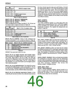
SYSTEM_CONFIG
TX_RATE_A,
(Write/Read Address)
TX_RATE_B
This is a Read/Write register (8 bits wide), which allows
the Watchdog Function to be enabled and disabled via
bit 9. Note that following a system reset this bit is set low,
thus enabling the watchdog.
(Write Address)
These are write registers for UARTsA and B, which allow
the Transmit baud rates to be set as shown in Table 32.
Other binary combinations of bit settings (not shown in
Table 32) are invalid and should not be used as the results
would be indeterminate.
Bit 9
Watchdog function
0
1
Enabled
Disabled
Bit setting
Transmit Baud rate
Table 34 Enabling the Watchdog function through the
SYSTEM_CONFIG register
11
10
9
8
0
0
0
0
0
0
0
0
1
0
0
0
0
1
1
1
1
0
0
0
1
1
0
0
1
1
0
0
1
0
1
0
1
0
1
0
300
600
Bits 5 to 10 and 13 are not used and could be set high or
low. The Chip revision number appears on bits 12 to 15
when read.
1200
2400
4800
9600
19·2k
38·4k
76·8k
SYSTEM_ERROR_STATUS
This is an 8-bit wide read only register, and allows the
source of a system reset to be determined via bits 11 to 8.
All bits are reset low after being read. The Chip revision
number appears on bits 12 to 15 when read.
Table 32 Transmit Baud rate settings in the TX_RATE_A
and TX_RATE_B registers
44

 ZARLINK [ ZARLINK SEMICONDUCTOR INC ]