GP2021
ACCUM_STATUS_A, ACCUM_STATUS_B, and
ACCUM_STATUS_C registers. Performing a write to
STATUS prior to reading the status registers ensures
reading of stable status values. The latch takes effect within
300ns of the trailing edge of the write pulse. The active
edge transition of the ACCUM_INT signal will also latch
the state of the status bits, thus it is not necessary to write
to STATUS when the status registers are to be read as a
response to theACCUM_INTsignal in an interrupt handling
routine. The write to STATUS is required only when the
status registers are read at times that are not synchronised
to the interrupts. These two mechanisms are mutually
exclusive and should not be used together; if both are used,
a write to STATUS soon after the occurrence of an
ACCUM_INT signal can result in confused readings. To
avoid conflict the INTERRUPT_ENABLE in the
SYSTEM_SETUP register should be set low if writes to
STATUS are to be used.
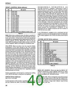
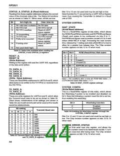
RESET_CONTROL (Write address)
Bit
Bit name
15
14
13
12
11
10
9
8
7
6
5
Not used
Not used
Not used
CH11_RSTB
CH10_RSTB
CH9_RSTB
CH8_RSTB
CH7_RSTB
CH6_RSTB
CH5_RSTB
CH4_RSTB
CH3_RSTB
CH2_RSTB
CH1_RSTB
CH0_RSTB
4
3
2
1
0
MRB, active low software master reset
If the INTERRUPT_ENABLE bit in SYSTEM_SETUP
register is set low, the interrupt will not latch the status bits
in the status registers, but a STATUS write access will do
so.
Table 24
MRB: When low (a software reset), the effect is similarlr to
a hardware reset except that the clock generator, the time
base generators, measurement data and peripheral
functions are not affected and the Status bitsACCUM_INT,
DISCIP, DISCIP_GLITCH, MEAS_INT, and TIC are not
reset. MRB should be set high to allow access to all of the
various registers. MRB is set high by a hardware reset.
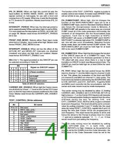
SYSTEM_SETUP (Write address)
Bit name
Bit
15
14
13
12
11
10
9
Not used
Not used
Not used
Not used
Not used
CHx_RSTB: When set active Low, the reset bit inhibits
propagation of the clock phases to the CHx tracking
channel and resets theAccumulated Data flags, Code DCO
and Carrier DCO accumulators, the I and Q accumulators,
and the Code Phase Counter.ACHx_RSTB does not reset
the Carrier Cycle, Code Slew or the Epoch counters. At
the end of the reset, the channel enable resets the code
generator to a previously programmed start phase. This is
all required for the parallel search algorithm of one satellite
signal using many channels in order to start from a known
relative code phase on all the channels. All of the control
registers in CHx can be programmed and read as usual
during the reset state. To restart normal operation in several
different channels at the same time, the corresponding
CHx_RSTB bits should be set high during the same write
operation. All CHx_RSTB are set low by a master reset,
(both hardware and software), so a write low to bit 0 of this
register will force a low onto bits 12 to 1 regardless of what
was previously on the bus.
MEAS_INT_SOURCE
OPS-DRIVE-SEL
8
IPS_3V_MODE
7
6
5
4
3
2
1
lNTERRUPT_PERIOD
FRONT_END_MODE
INTERRUPT_ENABLE
DISCOP_SELECT_100KHZ
DISCOP_SELECT TIMEMARK
DISCOP_SELECT_CH0_DUMP
DISCOP
0
CARRIER_MIX_DISABLE
Table 25
MEAS_INT_SOURCE: When set high the MEAS_INT
output is cleared by a read of MEAS_STATUS_A, when
low by a read of ACCUM_STATUS_B. A master reset
forces the MEAS_INT_SOURCE bit low.
Power consumption can be kept to a minimum by setting
CHx_RSTB Low when a channel is not required.
STATUS (Write Address)
OPS_DRIVE_SEL:When set high this control bit increases
the size of the output driver on ACCUM_INT, MEAS_INT,
and D<15:0> pins so as to increase the drive of these pins
if they are driving a large load. Master reset forces
OPS_DRIVE_SEL low.
Bits 15 to 0: not used
A write operation to this location, regardless of the data on
the bus, latches the state of all status bits contained in
40

 ZARLINK [ ZARLINK SEMICONDUCTOR INC ]