GP2021
The CHx_CODE_SLEW register can be written to at any
time. If two accesses have taken place before a DUMP in
U PDATE mode or before a TIC when in PRESET mode,
the latest value will be used at the next slew operation.
During the time a slew process is being executed, any
further write access to the CHx_CODE_SLEW register will
be stored until the following DUMP and then cause the
transfer of this new value into the counter. This situation
may be avoided by synchronising the access with the
associated CHx_NEW_ACCUM_DATA status bit.
released. This write will be acted on immediately the reset
is released.
If a TIC occurs during or soon after a slew the channel will
not be locked to the satellite, so the Measurement Data
for that channel will not be of use.
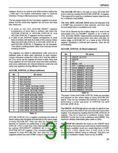
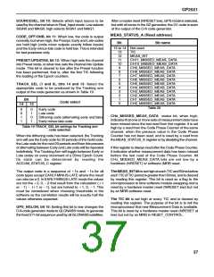
The ability to read the Slew counter is included only for
testing hardware or software and has no other use. It will
only give a non-zero result if the read occurs during the
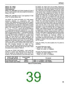
actual slew operation. An example of a slewing event is
shown in Fig.23.
If a channel is inactive, a non-zero slew value should be
written into CHx_CODE_SLEW before the channel is
1023 CHIPS
1025·5 CHIPS
DUMP
DUMP
DUMP
TIME
t
1
C/A CODE CHIP NO:
1021 1022 1023
1
1
1
1
2
3
t : Load 5 into CHx_CODE_SLEW register = 2·5 chips delay
1
Figure 23 Slew timing in UPDATE mode
CHx_EPOCH_CHECK (Read Address)
Bits 15 to 14: Not used.
value that was sampled at the last TIC event, with a valid
range from 0 to 19.
Bits 13 to 8: Instantaneous value of CHx_20MS_EPOCH.
Bits 7 to 5: Not used.
CHx_EPOCH_COUNT_LOAD
MULTI_EPOCH_COUNT_LOAD
ALL_EPOCH_COUNT_LOAD
(Write Address)
Bits 4 to 0: Instantaneous value of CHx_1MS_EPOCH.
Bits 15, 14, 7, 6, and 5: Not used.
Reading this address gives the instantaneous value of the
CHx_1MS_EPOCH and the CHx_20MS_EPOCH
counters. It can be used to verify if the Epoch counters
have been properly initialised by the software. Its value is
not latched and is incremented on each DUMP. To ensure
the correct result, this register should be read only when
there is no possibility of getting a DUMP during the read
cycle, by synchronising the read to NEW_ACCUM_DATA.
The ranges of these values are the same as those seen in
the CHx_EPOCH register.
Bits 13 to 8: CHx_20MS_EPOCH The value to be loaded
into the 20 millisecond epoch counter, with a valid range
from 0 to 49.
Bits 4to 0: CHx_1 MS_EPOCH Thevalue to be loaded
intothe 1 millisecond epoch counter, with a valid range from
0 to 19. This operation is affected by the current channel
mode, (PRESETor UPDATE). In UPDATE mode, the data
written into these registers is immediately transferred to
the 1ms and 20ms epoch counters. In PRESET mode
however, the data is transferred only after the next TIC.
CHx_EPOCH (Read Address)
Bits 15, 14, 7, 6 and 5: Not used. Read gives low.
It is important to load the CHx_EPOCH register last in the
PRESET mode loading sequence because the trailing
edge of a write to this register enables the whole PRESET
operation on the next TIC.
Bits 13 to 8: CHx_20MS_EPOCH The 20ms epoch
counter value that was sampled at the last TIC event, with
a valid range from 0 to 49.
Refer to Detailed Operation of the GP2021 for more details
of the PRESET mode on page 25
Bits4 to 0: CHx_1 MS_EPOCH The 1ms epoch counter
35

 ZARLINK [ ZARLINK SEMICONDUCTOR INC ]