GP2021
address, there is no need to wait 300ns before writing the
_LOW part. For further information refer to General
Interface Timing in Microprocessor Interface section.
The ACCUM_INT bit is set high at every ACCUM_INT
and is reset by reading the ACCUM_STATUS_A register.
This status bit is reset by a hardware master reset but not
by a software reset (MRB).
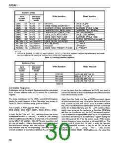
The bit assignments for the Correlator registers are given
below, but two write-only registers do not have any data
bits, these are:
The CHx_NEW_ACCUM_DATA status bit indicates that
a DUMP has occurred in that channel, and that new
Accumulated Data is available to be read.
1. A write to the CHx_ACCUM_RESET register
(irrespective of what data is written) will reset the
ACCUM_STATUS_A, ACCUM_STATUS_B, and
ACCUM_STATUS_C registers for that channel.
2. A write to the STATUS register (irrespective of what
data is written) will latch the state of the various status
flags into ACCUM_STATUS_A, ACCUM_STATUS_B
and ACCUM_STATUS_C Registers for all channels.
This allows a polling based rather than Interrupt driven
tracking scheme.
Each bit is cleared by the trailing edge of a read of the
associated CHx_Q_PROMPT register or by a write to
CHx_ACCUM_RESET. Note that the channel-specific bits
of this register will not show their new value until after an
active edge of ACCUM_INT or a write to the STATUS
register. Disabling a channel will however, clear the bit
immediately.
ACCUM_STATUS_B (Read address)
The registers are listed in alphabetical order and not in
address order to allow easy reference to each section.
Unless otherwise stated the LSB is bit 0 and the MSB is
bit 15 or as far up the register as there is data. Note that
most registers do not have both read and write functions,
and many addresses are shared between read-only and
write-only registers having different functions.
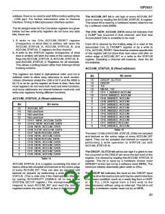
Bit name
DISCIP_GLITCH
DISCIP
TIC
MEAS_I NT
CH1 1_MISSED ACCUM
CH10_MISSED_ACCUM
CH9_MISSED_ACCUM
CH8_MISSED_ACCUM
CH7_MISSED_ACCUM
CH6_MISSED_ACCUM
CH5_MiSSED_ACCUM
CH4_MISSED_ACCUM
CH3_MISSED_ACCUM
CH2_MISSED_ACCUM
CH1_MISSED ACCUM
CH0_MISSED_ACCUM
Bit
15
14
13
12
11
10
9
8
7
6
5
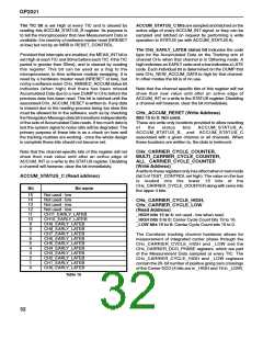
ACCUM_STATUS_A (Read address)
Bit
Bit name
15
14
13
12
11
10
9
8
7
6
5
ACCUM_INT
Not used-low
Not used-low
Not used-low
4
3
2
1
CH11_NEW_ACCUM_DATA
CH10_NEW_ACCUM_DATA
CH9_NEW_ACCUM_DATA
CH8_N EW_ACCU M_DATA
CH7_NEW ACCUM_DATA
CH6_NEW_ACCUM_DATA
CH5_NEW ACCUM_DATA
CH4_NEW_ACCUM_DATA
CH3_NEW_ACCUM_DATA
CH2_NEW_ACCUM_DATA
CH1_NEW_ACCUM_DATA
CH0_NEW_ACCUM_DATA
0
Table 15
The lower 12 bits ofACCUM_STATUS_B bits are sampled
and latched on the active edge of every ACCUM_INT
signal. They can be sampled and latched on request by
performing a write operation to STATUS (as with
ACCUM_STATUS A).
4
3
2
1
The DISCIP_GLITCH bit will be set high if a glitch-to-low
has occurred on the DISCIP pin since the last read of this
register. It is cleared by reading this ACCUM_STATUS_B
register. This bit is reset by a hardware master reset
(NRESET at low) but not by a software reset (MRB). The
minimum reliably detectable glitch width is 25ns.
0
Table 14
ACCUM_STATUS_A is a register containing the state of
twelve status bits sampled and latched on the active edge
of every ACCUM_INT. They can also be sampled and
latched on request, by performing a write operation to
STATUS. (This is safe only if the interrupts are stopped,
by setting INTERRUPT_ENABLE bit to low in the
SYSTEM_SETUP register.) The microprocessor must
respond to each ACCUM_INT and read the channel
registers before the next DUMP is due in that channel.
The DISCIP bit indicates the level on the DISCIP input
pin at the time this read occurs and may be used to interface
a hardware condition (such as a ready flag from a UART
or the PLL LOCK signal from a front end) to the
microprocessor without using an interrupt. This bit is not
reset by a hardware master reset nor by an MRB.
31

 ZARLINK [ ZARLINK SEMICONDUCTOR INC ]