GP2021
word. A 25-bit increment number is adequate for a 26-bit
accumulator DCO as the increment to the MSB is always
zero.
register and it can be written to at any time in PRESET
mode or in UPDATE mode, but only has effect when
PRESET mode is entered. The weight of the least
significant bit of PRESET phase is 2p/256 radians of a
half chip cycle.
The LSB of the INCR register represents a step given by:
Min. step frequency, Real_Input mode = (40MHz47)4226
In UPDATE mode this register has no use other than as
preparation for PRESET mode.
= 85·14949mHz
Refer to Detailed Operation of GP2021 for further
information on PRESET mode, page 25.
Min. stepfrequency, Complex_Inputmode=(35MHz46)4226
= 86·92344mHz
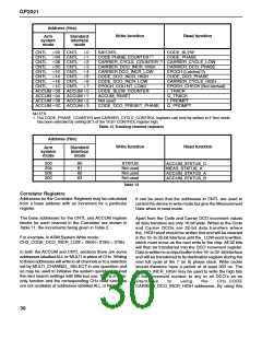
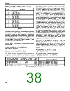
CHx_CODE_PHASE (Read Address)
CHx_CODE_PHASE_COUNTER,
MULTI_6ODE_PHASE_COUNTER,
ALL_CODE_PHASE_COUNTER
(Write Address)
Output frequency = CHx_CARRIER_DCO_INCR (min. step
frequency).
Note: The Code DCO drives the Code Generator to give
half chip time steps and so must be programmed to twice
the required chip rate. This means that the chip rate
resolution is 42·57475mHz in Real_lnput mode or
43·46172mHz in Complex_Input mode.
Bits 15 to 11: Not used, Low when read.
Bits 10 to 0: CHx_CODE_PHASE (Read)This is the state
of the Code Phase Counter, (an 11-bit binary up counter
clocked by the Code Generator Clock), stored on TIC.The
phase is expressed as a number of half code chips and
ranges from 0 to 2046 half chips. Areading of 2046 is very
rare and can only occur if theTIC captures the Code phase
just after the counter reaches 2046 and before it is reset
by a DUMP from the C/A Code Generator. DUMP also
increments the Epoch counter, so the meaning of a phase
value of 2046 1 the previous Epoch value is the same as
a phase value of 0 1 the incremented Epoch value, and
either is valid. If a TIC occurs during a Code Slew the
reading will be 0, and that channel’s Measurement Data is
of no use.
The nominal frequency is 1.023000000MHz before
allowing for Doppler shift or crystal error. Writing
016EA4A8H into the CHx_CODE_DCO_INCR register will
generate a chip rate of 1.022999968MHz in Real_lnput
mode. In Complex_mode, 01672922H will generate a chip
rate of 1.022999970 MHz.
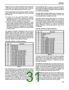
CHx_CODE_DCO_PHASE (Read Address)
Bits 15 to 10: Not used (low when read).
Bits 9 to 0: CHx_CODE_DCO_PHASE: Contains the ten
more significant bits (25 to 16) of the Code DCO phase
accumulator sampled at a TIC event. It is an unsigned
integer valid from 0 to 1023. The weight of the least
significant bit is 2p/1024 radians, 2p being half of a code
chip, so the pseudorange resolution is 1/2048 of a chip,
(equivalent to 0·15 metre or 0·5ns).
Bits 10 to 0: (Write) loads the 11 bits of the
CHx_CODE_PHASE_COUNTER. A write to these
registers is only possible in test mode, enabled by setting
the TM_TEST bit of TEST_CONTROL to High.
CHx_CODE_SLEW (Read Address)
CHx_CODE_SLEW_COUNTER,
MULTI_CODE_SLEW_COUNTER,
ALL_CODE_SLEW_COUNTER
(Write Address)
The CHx_CODE_DCO_PHASE content is not protected
by any overwrite protection mechanism.
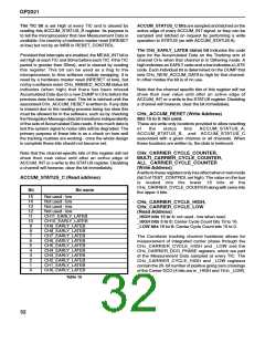
CHx_CODE_DCO_PRESET_PHASE,
MULTI_CODE_DCO_PRESET_PHASE,
ALL_CODE_DCO_PRESET_PHASE
(Write Address)
Bits 15 to 11: Not used.
Bits 10 to 0: An unsigned integer ranging from 0 to 2047
representing the number of code half chips to be slewed
immediately after the next DUMP if in UPDATE mode
orafter the next TIC, if in PRESET mode. Since there are
only 2046 half chips in a GPS C/A code, a programmed
value of 2047 is equivalent to a programmed value of 1,
but the next DUMP event will take place 1ms later. In
PRESET mode, the slew timing is set only by TIC, which
will also reset the code generator, (no DUMP is needed).
A non-zero slew must always be programmed when using
PRESET mode.
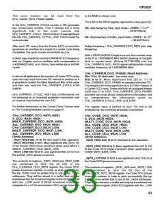
Bits 15 to 8: Not used.
Bits 7 to 0: More significant bits (25 to 18) of the Code
DCO phase which is to be loaded at the next TIC event in
PRESET mode.
In PRESET mode, the 8 bits of the CHx_CODE
_DCO_PRESET_PHASE register, with zeros filling the
lower bits, are transferred to the CODE DCO accumulator
on the nextTIC. The previous accumulator phase is totally
overwritten. The PRESET_PHASE register is a write-only
34

 ZARLINK [ ZARLINK SEMICONDUCTOR INC ]