GP2021
The cycle fraction can be read from the
CHx_Carrier_DCO_Phase register.
to the MSB is always zero.
The LSB of the INCR register represents a step given by:
In the CHx_CARRIER_CYCLE counter, a TIC generates
two consecutive actions. First it latches the 4 more
significant bits of the cycle counter into
CHx_CARRIER_CYCLE_HIGH and the 16 less significant
bits into CHx_CARRIER_CYCLE_LOW.Then it resets the
cycle counter.
Min. step frequency, Real_Input mode = (40MHz47)4227
= 42·57475mHz
Min. stepfrequency, Complex_Inputmode=(35MHz46)4227
= 43·46172mHz
After each TIC, every time the Carrier DCO accumulator
generates an overflow as a result of a carrier cycle being
completed, the cycle counter increments by one.
Output frequency = CHx_CARRIER_DCO_INCR (min. step
frequency).
With a GP2015/GP2010 style front end, the nominal value
of the IF is 1·405396826 MHz before allowing for Doppler
shift or crystal error. Writing 01F7B1B9H into the
CHx_CARRIER_DCO_INCR register will generate a local
oscillator frequency of 1·405396845 MHz.
In Real_lnput mode the nominal CARRIER DCO frequency
with no Doppler and no oscillator drift compensation is
1·405396825 MHz, so in 100ms, there will be about 140540
cycles.
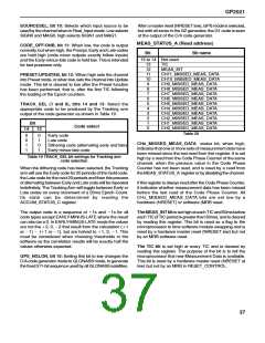
CHx_CARRIER_DCO_PHASE (Read Address)
Bits 15 to 10: Not used - low when read.
In almost all applications the number of Carrier DCO cycles
does not vary much from one TIC interval to another so it
is possible to predict the Most Significant Bits of the value
and then only read the CHx_CARRIER_CYCLE_LOW
register.
Bits 9 to 0: More significant bits (26 to 17) of
CHx_CARRIER_DCO_PHASE as sampled at the lastTIC.
The weight of the least significant bit is 2p/1024 radians of
a Carrier DCO cycle. These bits form an unsigned integer
valid from 0 to 1023. CHx_CARRIER_DCO_PHASE
provides sub-cycle phase measurement information and
so complements the information given by
CHx_CARRIER_CYCLE_HIGH and_LOW.
CHx_CARRIER_CYCLE_HIGH and_LOWcontents are
not protected by an overwrite protection mechanism and
so must be read before the next TIC.
For further information on the Carrier Cycle Counter refer
to The Tracking Modules section on page 8.
The register value is latched on each TIC and is not
protected by any overwrite protection mechanism.
CHx_CARRIER_DCO_INCR_HIGH,
X_DCO_INCR_HIGH,
CHx_CODE_DCO_INCR_HIGH,
X_DCO_INCR_HIGH,
MULTI_CARRIER_DCO_INCR_HIGH,
ALL_CARRIER_DCO_INCR_HIGH,
CHx_CARRIER_DCO_INCR_LOW,
MULTI_CARRIER_DCO_INCR_LOW,
ALL_CARRIER_DCO_INCR_LOW
(Write Address)
_INCR_HIGH bits 15 to 10: Not used in this operation.
_INCR_HIGH bits 9 to 0: More significant bits (25 to 16)
of the Carrier DCO phase increment when used before a
write to _CARRIER_DCO_INCR_LOW.
_INCR_LOW bits 15 to 0:Less significant bits (15 to 0) of
the Carrier_DCO (phase increment.
MULTI_CODE_DCO_INCR_HIGH,
ALL_CODE_DCO_INCR_HIGH,
CHx_CODE_DCO_INCR_LOW,
MULTI_CODE_DCO_INCR_LOW,
ALL_CODE_DCO_INCR_LOW
(Write Address)
_INCR_HIGH bits 15 to 9: Not used in this operation.
_INCR_HIGH bits 8 to 0: More significant bits (24 to 16)
of the Code DCO phase increment when used before a
CODE_DCO_INCR_LOW.
_INCR_LOW bits 15 to 0: Less significant bits (15 to 0) of
the Code DCO phase increment.
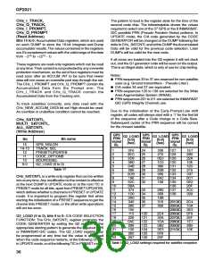
The contents of registers _INCR_HIGH and_lNCR_LOW
are combined to form the 26 bits of the
CHx_C,ARRIER_DCO_INCR register, the carrier DCO
phase increment number. In order to write successfully,
the top 10 bits must be written first, to any of the _HIGH
addresses. They will be stored in a buffer and only be
transferred into the increment register of the DCO together
with the _LOW word. A 26-bit increment number is
adequate for a 27-bit accumulator DCO, as the increment
The contents of registers _INCR_HIGH and _INCR_LOW
are combined to form the 25 bits of the
CHx_CODE_DCO_INCR register, the Code DCO phase
increment number. In order to write successfully, the top
9 bits must be written first, to any of the _HIGH addresses.
They will be stored in a buffer and only be transferred into
the increment register of the DCO together with the _LOW
33

 ZARLINK [ ZARLINK SEMICONDUCTOR INC ]