GP2021
Address (Hex)
Write function
Read function
Arm
system
mode
Standard
interface
mode
CNTL 100
CNTL 104
CNTL 108
CNTL 10
CNTL 11
CNTL 12
SATCNTL
CODE PHASE COUNTER (1)
CARRIER_CYCLE_COUNTER (1) CARRIER_CYCLE_LOW
CODE_SLEW
CODE_PHASE
CNTL 10C CNTL 13
CARRIER_DCO_INCR_HIGH
CARRIER DCO_INCR_LOW
CODE_DCO_INCR_HIGH
CODE_DCO_INCR_LOW
EPOCH_COU NT_LOAD
CODE_SLEW_COUNTER
ACCUM_RESET
CARRIER_DCO_PHASE
EPOCH (Latched 0)
CODE_DCO_PHASE
CARRIER_CYCLE_HIGH
EPOCH_CHECK (Not latched)
I_TRACK
CNTL 110
CNTL 114
CNTL 118
CNTL 14
CNTL 15
CNTL 16
CNTL 11C CNTL 17
ACCUM100
ACCUM104
ACCUM108
ACCUM10
ACCUM11
ACCUM12
Q_TRACK
l_PROMPT
Not used
ACCUM10C ACCUM13
CODE_DCO_PRESET_PHASE
Q_PROMPT
NOTES
1. The CODE_PHASE_COUNTER and CARRIER_CYCLE_CONTROL registers can only be written to if Test mode
has been selected by setting bit 3 of the TEST CONTROL register high.
Table 12 Tracking channel registers
Address (Hex)
Write function
Read function
Arm
system
mode
Standard
interface
mode
200
204
208
20C
80
81
82
83
STATUS
Not used
Not used
Not used
ACCUM_STATUS_C
MEAS_STATUS_A
ACCUM_STATUS_A
ACCUM_STATUS_B
Table 13
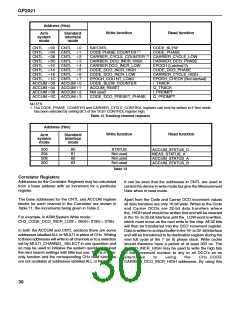
Correlator Registers
Addresses for the Correlator Registers may be calculated
from a base address with an increment for a particular
register.
It can be seen that the addresses in CNTL are used to
control the device in write mode but give the Measurement
Data when in read mode.
The base addresses for the CNTL and ACCUM register
blocks for each channel in the Correlator are shown in
Table 11, the increments being given in Table 2.
Apart from the Code and Carrier DCO increment values
all data transfers are only 16-bit wide. Writes to the Code
and Carrier DCOs are 32-bit data transfers where
the_HIGH word should be written first and will be retained
in the 16- to 32-bit interface until the _LOW word is written,
which must occur as the next write to the chip. All 32 bits
will then be transferred into the DCO increment register.
Data is written to an input buffer in the 16- to 32- bit interface
and will be transferred to its destination register during the
next full cycle of the 7 (or 6) phase clock. Write cycles
should therefore have a period of at least 300 ns. The
X_DCO_INCR_HIGH may be used to write the high bits
of the increment number to any or all DCO’s as an
For example, in ARM System Write mode:
CH3_CODE_DCO_INCR_LOW = 060H1018H = 078H.
In both the ACCUM and CNTL sections there are some
addresses labelledALL or MULTI in place of CHx. Writing
to these addresses will write to all channels or to a selection
set by MULTI_CHANNEL_SELECT in one operation and
so may be used to initialise the system quickly or to load
the next search settings with little bus use. This is a write-
only function and the corresponding CHx read functions
are not available at addresses labelled ALL or MULTI.
alternative
to
using
the
CHx_CODE
CARRIER_DCO_INCR_HIGH addresses. By using this
30

 ZARLINK [ ZARLINK SEMICONDUCTOR INC ]