GP2021
to UTC, the internal TIMEMARK will be within 100ns
(4/73175ns) of UTC in Real_lnput mode or 85·7ns
(3/63171.4ns) of UTC in Complex_lnput mode. In addition,
there may be a delay of up to 50ns in getting the
TIMEMARK output off chip, giving a maximum error of
150ns (Real_lnput) or 135·7ns (Complex_lnput) between
TIMEMARK and UTC. It should be noted that due to the
need to re-synchronise TIC, a jitter of up to 175ns may be
present on TIMEMARK, along with any jitter and drift
present on the input clock. The pulse width of TIMEMARK
(in seconds) is either (571412/7)3(7/ Master Clock
Frequency) for Real_lnput mode giving 1·0000000ms
(assuming an accurate 40MHz master clock input) or
(583311/6)3(6/Master Clock Frequency) for
Complex_lnput mode giving 0·9999714ms (assuming an
accurate 35MHz master clock input).
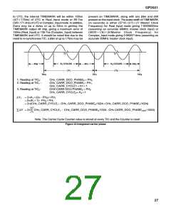
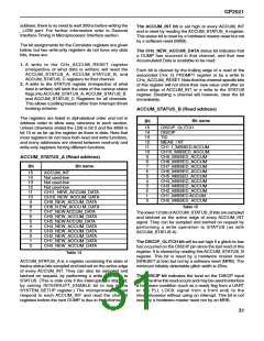
K
1
CYCLES
K CYCLES
2
PH
0
PH
1
PH
2
DY
1
DY
2
TIC
TIC
TIC
2
0
1
1. Reading at TIC0:
2. Reading at TIC1 :
CHx_CARR_DCO_PHASE0 = PH0
CHx_CARR_DCO_PHASE1= PH1
CHx_CARR_CYCLE1 = K111
CHX-CARR-DCO-PHASE2 = PH2
CHx_CARR_CYCLE2 = K211
3. Reading at TIC2:
DY1 = 2pK11(2p2PH0)1PH1
= 2p(K111)2PH01PH1
= 2p(CHx_CARR_CYCLE12CHx_CARR_DCO_PHASE0/10241CHx_CARR_DCO_PHASE1/1024)
LAST
LAST/1024)
SDY = 2pSCHx_CARR_CYCLE 2 CHx_CARR_DCO_PHASE /10242CHx CARR_DCO_PHASE
1
0
i = 1
Note: The Carrier Cycle Counter value is stored at every TIC and the Counter is reset
Figure 22 Integrated carrier phase
27

 ZARLINK [ ZARLINK SEMICONDUCTOR INC ]