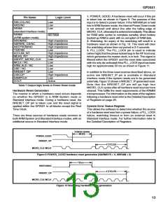
GP2021
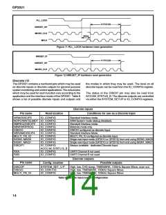
ARM System Mode
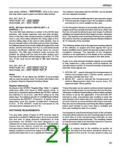
ARM System Mode, as shown in Figure 14, allows
the GP2021 to be interfaced with an ARM60
microprocessor and external memory devices (i.e RAM,
ROM, EEPROM, EPROM, Flash) without the need for
external glue logic.
and the control signalsARM_ALE and DBE to match the
timing requirements of the various memory devices .
The memory interface is via the memory chip select lines
(NRAM, NEEPROM, NROM and NSPARE_CS), the Read
line (NRD) and the byte write select outputs (NW<3:0>).
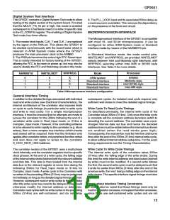
Address Map
Both the GP2021 and external memory devices are
memory mapped into 1Mbyte segments by A<22:20> as
shown in Table 10.
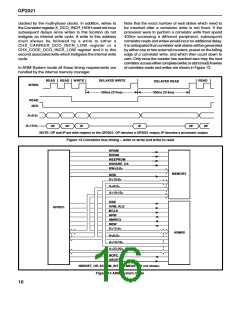
ARM System Timing
The GP2021 timing diagrams for each of the memory
interfaces (EEPROM, RAM, ROM, SPARE), and ARM60
are shown in the Electrical Characteristics.
Decoded
Device
A22 A21 A20
output pin
selected
Wait State Generation
To allow access to slow peripherals or memory, the clock
(MCLK) to the ARM60 microprocessor may be stretched
in either Phase 1 (low) or Phase 2 (high), thus allowing
wait states to be introduced (where a wait state is defined
as being one MCLK period).
0
0
0
0
1
1
1
1
0
0
1
1
0
0
1
1
0
1
0
1
0
1
0
1
ROM
RAM
Correlator
Support functions
EEPROM
User defined
Not decoded
Not decoded
NROM
NRAM
NEEPROM
NSPARE_CS
The GP2021 introduces one wait state for accesses to the
RealTime Clock, Dual UARTand System Control registers,
as shown in Figure 15. Correlator accesses as shown in
Figure 19 incur one wait state; subsequent accesses being
prevented from contravening the Correlator requirements
(see Correlator Functional Description) by adding several
wait states.
Table 10 ARM system address map
TheARM60 is able to perform either byte or word (4 bytes
wide) writes to memory. All registers within the GP2021
are word aligned, with only write accesses to external RAM
being either byte or word aligned. The signal NBW is used
to indicate either a byte or word write request, withA<1:0>
performing byte selection.
In order to ensure compatibility with a variety of memory
devices, the ROM interface is programmable with between
one to three wait states, while the EEPROM and SPARE
interfaces can be programmed with between three to six
wait states via the Wait State Register.
Decoding of NBW and A<1:0> is performed by the
Microprocessor Interface, with NW<3:0> being the byte
write select outputs to memory. During a word write all
four of the outputs NW<3:0> will be active.
For further information on the Wait State Register, refer to
Detailed Description of Registers. Read and write cycles
for the RAM, EEPROM (or Spare) and ROM interfaces
are shown in Figures 16 through18.
Note that the register addresses for the Correlator and
Support Functions are as shown in the GP2021 Register
Map.
During a read cycle from Flash memory, the output disable
to data bus release time, could be greater than 25ns. Hence
in order to avoid bus contention, the nominal period of
MCLK is stretched by 25ns during the following cycle.
Control Signals
The GP2021 uses the ARM60 control signals NBW,
NMREQ and NRW to generate the processor clock MCLK
17

 ZARLINK [ ZARLINK SEMICONDUCTOR INC ]