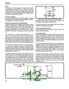
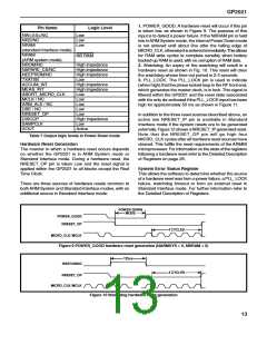
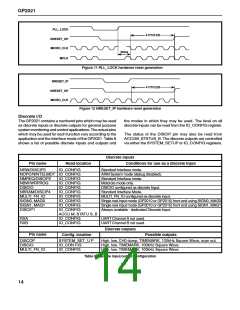
GP2021
clocked by the multi-phase clocks. In addition, writes to
the Correlator register X_DCO_INCR_HIGH need not incur
subsequent delays since writes to this location do not
instigate an internal write cycle. A write to this address
must always be followed by a write to either a
CHX_CARRIER_DCO_INCR_LOW register or a
CHX_CODE_DCO_INCR_LOW register and it is this
second associated write which instigates the internal write
cycle.
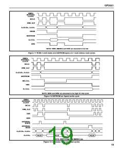
Note that the exact number of wait states which need to
be inserted after a correlator write is not fixed. If the
processor were to perform a correlator write then spend
400ns accessing a different peripheral, subsequent
correlator reads and writes would incur no additional delay.
It is anticipated that correlator wait states will be generated
by either one or two external counters, preset on the falling
edge of a correlator write, and which then count down to
zero. Only once the counter has reached zero may the next
correlatoraccesseithercomplete(write)orstart(read)Aseries
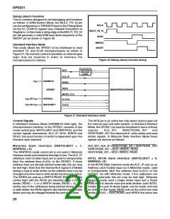
of correlator reads and writes are shown in Figure 13.
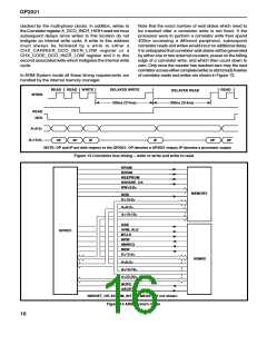
In ARM System mode all these timing requirements are
handled by the internal memory manager.
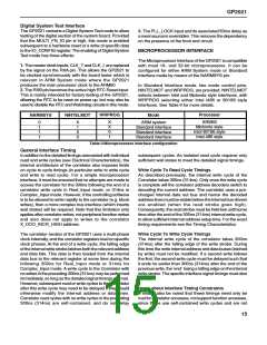
READ
READ WRITE
DELAYED WRITE
300ns (314ns)
READ
DELAYED READ
300ns (314ns)
WREN
READ
NCS
A<9:2>
D<15:0>
0P
0P
IP
IP
0P
0P
NOTE: OP and IP are with respect to the GP2021. OP denotes a GP2021 output, IP denotes a processor output
Figure 13 Correlator bus timing – write to write and write to read
NRAM
NROM
NEEPROM
NSPARE_CS
NW<3:0>
MEMORY
NRD
D<15:0>
A<9:2>
A<19:10>
DBE
ARM_ALE
MCLK
GP2021
NRW
NMREQ
NBW
D<15:0>
ARM60
A<9:2>
A<19:10>
A<22:20>, A<1:0>
NOPC
ABORT
NRESET_OP, ACCUM_INT and MEAS_INT not shown
Figure 14 ARM system mode
16

 ZARLINK [ ZARLINK SEMICONDUCTOR INC ]