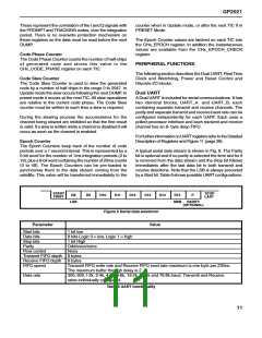
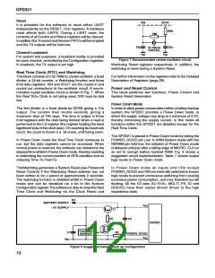
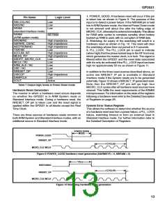
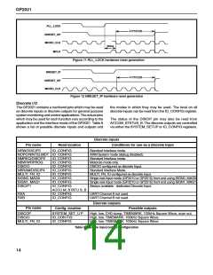
GP2021
Digital System Test Interface
The GP2021 contains a Digital System Test mode to allow
testing of the digital section of the system board. Provided
that the MULTI_FN_IO pin is high, this mode is enabled
subsequent to a hardware reset or a write of specific data
to the IO_CONFIG register. The enabling of Digital System
Test mode has three effects:
3. The PLL_LOCK input and its associated 50ms delay as
a reset source is overridden. This removes the dependency
on the presence of the front end circuit.
MICROPROCESSOR INTERFACE
The Microprocessor Interface of the GP2021 is compatible
with most 16- and 32-bit microprocessors. It can be
configured for either ARM System mode or Standard
Interface mode by means of the NARMSYS pin.
1. The master clock inputs, CLK_Tand CLK_I, are replaced
by the signal on the RXA pin. This allows the GP2021 to
be clocked synchronously with the board tester which is
relevant in ARM System mode where the GP2021
produces the main processor clock to the ARM60.
2.The RXB pin becomes the active high RTC Reset input.
This is mainly intended for factory testing of the GP2021,
allowing the RTC to be reset on power up, but may also be
used to disable the RTC and Watchdog circuits in this mode.
In Standard Interface mode, two mode control pins,
NINTELMOT and WRPROG, are provided. NINTELMOT
selects between Intel and Motorola style interfaces, with
WRPROG selecting either Intel i486 or 80186 style
interfaces. See Table 9 for more details.
WRPROG
Processor
NARMSYS
NINTELMOT
Mode
X
X
0
1
ARM60
0
1
1
1
X
1
0
0
ARM system
Motorola style
Intel 80186 style
Intel 486 style
Standard interface
Standard interface
Standard interface
Table 9 Microprocessor interface configuration
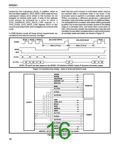
General Interface Timing
In addition to the detailed timings associated with individual
read and write cycles (see Electrical Characteristics), the
internal architecture of the correlator also imposes limits
on cycle to cycle timings (in particular write to write cycle
and write to read cycle). For a simple microprocessor
interface, it must be ensured that no attempts are made to
access the correlator for the 300ns following the end of a
correlator write cycle in Real_lnput mode, or 314ns in
Complex_lnput mode. However, if the controlling software
is to be allowed to write rapidly to the correlator (e.g. block
writes), then a more complex bus interface (which inserts
wait states) will be required. Note that this limitation only
applies after correlator writes, not peripheral function writes
and also does not apply to writes to the correlator
X_DCO_INCR_HIGH address.
subsequent cycles. An isolated read cycle requires only
sufficient wait states to meet the detailed signal timings.
Write Cycle To Read Cycle Timings
As described previously, the internal write cycle of the
Correlator takes 300ns (314ns). Only once the write cycle
is complete will the correlator address decoders switch to
decoding the current address. The correlator uses a pre-
charged internal data out bus and hence the decoded
address lines must be stable before the internal bus drivers
are enabled (when the read strobe goes high).
Consequently, the read strobe must be held low until some
time after the end of the 300ns (314ns) internal write cycle,
to allow sufficient internal address setup time. For the exact
timing requirements see the Timing Characteristics.
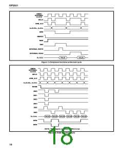
The correlator section of the GP2021 uses a multi-phase
clock internally, and the correlator registers load on specific
clock phases. At the end of a write cycle, the falling edge
of the internal write strobe latches both the relevant address
and data bits. This data is then loaded from the internal
data bus to the relevant register at some time during the
following 300ns for Real_lnput mode or 314ns for
Complex_lnput mode. A write cycle to the Correlator with
no writes in the preceding 300ns (314ns) may be performed
immediately, so long as the detailed signal timings are met.
However, subsequent read or write cycles to the Correlator
after this write cycle may need to be delayed if they would
otherwisw modify the internal address or data lines.
Correlator read cycles with no write cycles in the preceding
300ns (314ns) are self-contained, and do not delay
Write Cycle To Write Cycle Timings
The internal write cycle of the correlator takes 300ns
(314ns) after the falling edge of the write strobe. During
this time the write internal address and data buses (latched
by write) must not be modified. If a second write follows
the first, the second write cycle must be delayed such that
it ends no earlier than 300ns (314ns) after the end of the
previous write, the ‘end’ being a falling edge on the internal
write strobe. The specific interface signal timings must also
be met.
Notes about Interface Timing Constraints
It should also be noted that these timings need only be
met for correlator accesses, not support function accesses,
since these use self-contained write cycles and are not
15

 ZARLINK [ ZARLINK SEMICONDUCTOR INC ]