GP2021
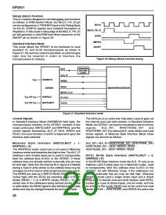
Debug (Abort) Function
This is a feature designed to aid debugging and functions
as follows: ln ARM System Mode, the MULTI_FN_IO pin
can be configured as a TRIGGER input to the Debug block
via the IO_CONFIG register (see Detailed Description of
Registers). In this mode a rising edge at the MULTI_FN_IO
pin will generate a valid ARM data Abort sequence at the
ABORT pin as shown in Figure 20.
MCLK
MULTI_FN_IO
NOPC
NMREQ
ABORT
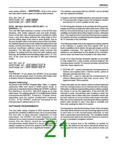
Standard Interface Mode
This mode allows the GP2021 to be interfaced to most
standard 16- and 32-bit microprocessors as shown in
Figure 21. No memory control is provided, so external glue
logic may be required in order to interface the
microprocessor to memory.
Figure 20 Debug (Abort) function timing
ADDRESS
DECODE
LOGIC
NCS
ALE_IP
WREN
V
DD
NARMSYS
GP2021
READ
MICROPROCESSOR
MICRO_CLK
D<15:0>
V
V
OR V
OR V
WRPROG
DD
SS
NINTELMOT
A<9:2>
DD
SS
Figure 21 Standard interface mode
Control Signals
The NCS pin is an active low chip select used to gate out
the internal read and write strobes. In Standard Interface
Mode, the GP2021 can best be visualised in terms of three
In Standard Interface Mode (NARMSYS held high), the
microprocessor interface of the GP2021 consists of two
mode control pins, NINTELMOT and WRPROG, and the
control signals themselves, ALE_IP, NCS, WREN and
READ, the exact function of which is dependent upon the
interface style selected.
signals,
ALE_INT,
WRSTROBE_INT
and
RDSTROBE_INT, the internalALE, write strobe and read
strobe signals. In Motorola Style Interface Mode these
signals are derived as follows:
Motorola Style Interface (NINTELMOT = 1,
WRPROG = X)
ALE_INT= ALE_IP•(WRSTROBE_INT+RDSTROBE_INT)
WRSTROBE_INT = NCS • WREN • READ
The WRPROG mode control pin is not used in Motorola
Interface mode and should be tied high or low.TheALE_IP
(Address Latch Enable input) pin is used to transparently
latch the address lines A<9:2> to the GP2021. If these
address lines are already latched externally, this pin may
be tied high. Note that the internal ALE signal is inhibited
during a read or write strobe so the address lines may be
changed once the read or write strobe has become active.
The WREN pin acts as a WRITE/READ ENABLE strobe
(active high) with the READ pin selecting either a READ
strobe (READ = 1) or a WRITE strobe (READ = 0). In a
similar way to the addresses being latched during a read
or write strobe, the READ signal is also latched during a data
strobe and may be changed towards the end of the cycle.
RDSTROBE_INT = NCS • WREN • READ
INTEL 80186 Style Interface (NINTELMOT = 0,
WRPROG =’0')
In the 80186 Style Interface mode the ALE_IP acts as an
Address Latch Enable input (as in Motorola mode), used
to transparently latch the address lines A<9:2> to the
GP2021. As with Motorola mode, if the addresses are
latched externally this pin may be tied high. Whereas
Motorola mode used a single strobe input and a Read/
Write level to denote read and write strobes, both INTEL
modes use a pair of strobe inputs, one for reads, and one
for writes. In this mode, READ acts as the active low read
strobe ( READ = RDSTROBE) and WREN the active low
20

 ZARLINK [ ZARLINK SEMICONDUCTOR INC ]