GP2021
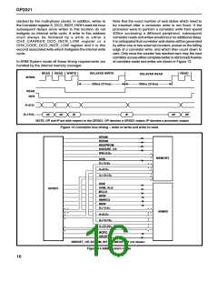
1. POWER_GOOD. A hardware reset will occur if this pin
is taken iow, as shown in Figure 9. The purpose of this
input is to detect a power failure. If the NBRAM pin is held
iow inARM System mode, the internal Power Down mode
is not entered until about 6ns after the falling edge of
MICRO_CLK, otherwiseit is entered immediately. Thisallows
for RAM write cycles to complete sensibly when battery
backed-up RAM is used, with no corruption of RAM data.
2. Watchdog. An expiry of the watchdog will result in a
hardware reset as shown in Fig. 10. This reset will clear
the watchdog whose time-out period is 2-3 seconds.
3. PLL_LOCK. The PLL_LOCK pin is used to indicate
(when high),that the phase locked loop in the RF front end,
which generates the master clock, is in lock. This signal is
filtered within the GP2021 and the reset state associated
with it is only de-activated if the PLL_LOCK input has been
high for approximately 50 ms as shown in Figure 11.
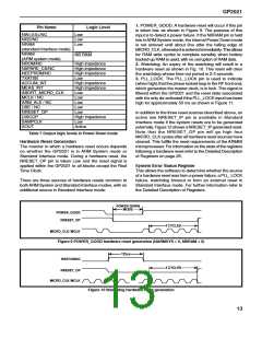
Pin Name
NW<3:0>/NC
NRD/NC
NRAM
(standard interface mode)
NRAM
(ARM system mode)
NROM/NC
NSPARE_CS/NC
NEEPROM/NC
TXATXB
ACCUM_INT
MEAS_INT
Logic Level
Low
Low
Low
NB RAM
High impedance
High impedance
High impedance
Low
High impedance
High impedance
Low
ABORT_MICRO_CLK
MCLK / NC
ARM_ALE / NC
DBE / NC
Low
Low
Low
NRESET_OP
DISCOP
SAMPCLK
Low
High Impedance
Low
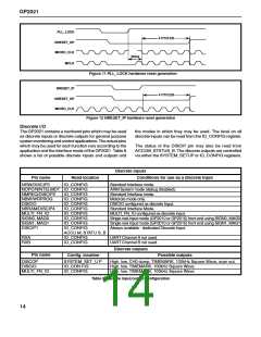
In addition to the three reset sources described above, an
active low NRESET_IP pin is available in Standard
Interface mode if the system resets are to be generated
externally. Figure 12 shows a NRESET_IP generated reset.
Note that the NRESET_OP pin will go high four
MICRO_CLK cycles after all hardware reset sources have
cleared. This fulfills the reset requirements of the ARM60
microprocessor. For information on the state of the registers
following a hardware reset refer to the Detailed Description
of Registers on page 28.
XOUT
Active
Table 7 Output logic levels in Power Down mode
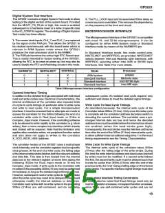
Hardware Reset Generation
The manner in which a hardware reset occurs depends
on whether the GP2021 is in ARM System mode or
Standard Interface mode. During a hardware reset, the
NRESET_OP pin is taken Low and the reset signal is
applied within the GP2021 to all blocks except the Real
Time Clock.
System Error Status Register
This allows the software to determine whether the source
of a hardware reset was from a power failure, a PLL_LOCK
failure, watchdog timeout or from an external reset in
Standard Interface mode. For further information refer to
the Detailed Description of Registers.
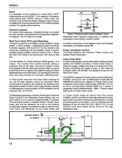
There are three sources of hardware resets common to
bothARM System and Standard Interface modes, with an
additional source in Standard Interface mode:
POWER DOWN
MODE
POWER_GOOD
NRESET_OP
4 CYCLES
MICRO_CLK/MCLK
Figure 9 POWER_GOOD hardware reset generation (NARMSYS = 0, NBRAM = 0)
122µs
WATCHDOG
4 CYCLES
NRESET_OP
MICRO_CLK/MCLK
Figure 10 Watchdog hardware reset generation
13

 ZARLINK [ ZARLINK SEMICONDUCTOR INC ]