R
QPRO XQ4000E/EX QML High-Reliability FPGAs
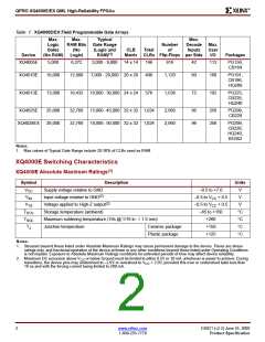
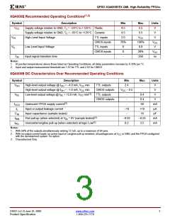
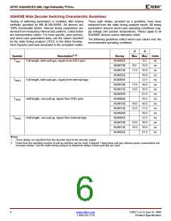
XQ4000E Wide Decoder Switching Characteristic Guidelines
Testing of switching parameters is modeled after testing
methods specified by MIL-M-38510/605. All devices are
100% functionally tested. Internal timing parameters are
derived from measuring internal test patterns. Listed below
are representative values. For more specific, more precise,
and worst-case guaranteed data, use the values reported
by the static timing analyzer (TRCE in the Xilinx Develop-
ment System) and back-annotated to the simulation netlist.
These path delays, provided as a guideline, have been
extracted from the static timing analyzer report. All timing
parameters assume worst-case operating conditions (sup-
ply voltage and junction temperature). Values apply to all
XQ4000E devices unless otherwise noted.
The following guidelines reflect worst-case values over the
recommended operating conditions.
-3
-4
(1,2)
Symbol
Description
Device
Max
Max
9.5
Units
ns
ns
ns
ns
ns
ns
ns
ns
ns
ns
ns
ns
ns
ns
ns
ns
T
Full length, both pull-ups, inputs from IOB I-pins
XQ4005E
XQ4010E
XQ4013E
XQ4025E
XQ4005E
XQ4010E
XQ4013E
XQ4025E
XQ4005E
XQ4010E
XQ4013E
XQ4025E
XQ4005E
XQ4010E
XQ4013E
XQ4025E
-
WAF
9.0
15.0
16.0
18.0
12.5
18.0
19.0
21.0
10.5
16.0
17.0
19.0
12.5
18.0
19.0
21.0
11.0
-
T
Full length, both pull-ups, inputs from internal logic
Half length, one pull-up, inputs from IOB I-pins
Half length, one pull-up, inputs from internal logic
-
11.0
13.0
-
WAFL
T
-
WAO
10.0
12.0
-
T
-
WAOL
12.0
14.0
-
Notes:
1. These delays are specified from the decoder input to the decoder output.
2. Fewer than the specified number of pull-up resistors can be used, if desired. Using fewer pull-ups reduces power consumption but
increases delays. Use the static timing analyzer to determine delays if fewer pull-ups are used.
6
www.xilinx.com
DS021 (v2.2) June 25, 2000
1-800-255-7778
Product Specification

 XILINX [ XILINX, INC ]