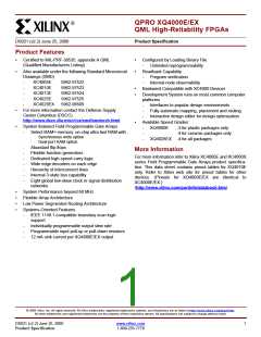
R
QPRO XQ4000E/EX QML High-Reliability FPGAs
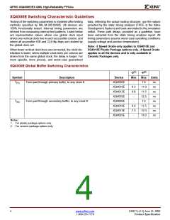
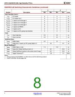
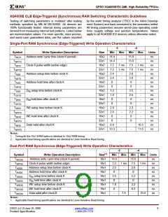
XQ4000E Horizontal Longline Switching Characteristic Guidelines
Testing of switching parameters is modeled after testing
methods specified by MIL-M-38510/605. All devices are
100% functionally tested. Internal timing parameters are
derived from measuring internal test patterns. Listed below
are representative values. For more specific, more precise,
and worst-case guaranteed data, use the values reported
by the static timing analyzer (TRCE in the Xilinx Develop-
ment System) and back-annotated to the simulation netlist.
These path delays, provided as a guideline, have been
extracted from the static timing analyzer report. All timing
parameters assume worst-case operating conditions (sup-
ply voltage and junction temperature). Values apply to all
XQ4000E devices unless otherwise noted.
The following guidelines reflect worst-case values over the
recommended operating conditions.
-3
-4
Symbol
Description
Device
Max
Max
Units
TBUF Driving a Horizontal Longline (LL):
T
T
I going High or Low to LL going High or Low, while T is Low.
Buffer is constantly active.
XQ4005E
XQ4010E
XQ4013E
XQ4025E
XQ4005E
XQ4010E
XQ4013E
XQ4025E
XQ4005E
XQ4010E
XQ4013E
XQ4025E
XQ4005E
XQ4010E
XQ4013E
XQ4025E
XQ4005E
XQ4010E
XQ4013E
XQ4025E
XQ4005E
XQ4010E
XQ4013E
XQ4025E
-
6.4
7.2
-
5.0
8.0
ns
ns
ns
ns
ns
ns
ns
ns
ns
ns
ns
ns
ns
ns
ns
ns
ns
ns
ns
ns
ns
ns
ns
ns
IO1
IO2
(1)
9.0
11.0
6.0
I going Low to LL going from resistive pull-up High to active Low.
-
(1)
TBUF configured as open-drain.
6.9
7.7
-
10.5
11.0
12.0
7.0
T
T going Low to LL going from resistive pull-up or floating High to
active Low. TBUF configured as open-drain or active buffer with
-
ON
7.3
7.5
-
8.5
(1)
I = Low.
8.7
11.0
1.8
T
T
T
T going High to TBUF going inactive, not driving LL.
-
OFF
PUS
PUF
1.5
1.5
-
1.8
1.8
1.8
T going High to LL going from Low to High, pulled up by a single
-
23.0
29.0
32.0
42.0
10.0
13.5
15.0
18.0
(1)
resistor.
22.0
26.0
-
T going High to LL going from Low to High, pulled up by two
-
(1)
resistors.
11.0
13.0
-
Notes:
1. These values include a minimum load. Use the static timing analyzer to determine the delay for each destination.
DS021 (v2.2) June 25, 2000
www.xilinx.com
5
Product Specification
1-800-255-7778

 XILINX [ XILINX, INC ]