R
QPRO XQ4000E/EX QML High-Reliability FPGAs
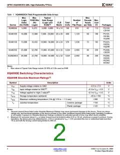
Table 1: XQ4000E/EX Field Programmable Gate Arrays
Max.
Logic
Gates
Max.
RAM Bits
(No
Typical
Max.
Decode
Inputs
Gate Range
(Logic and
Number
of
Max.
User
I/O
CLB
Total
(1)
Device
(No RAM)
Logic)
RAM)
Matrix CLBs Flip-Flops per Side
Packages
XQ4005E
5,000
6,272
3,000 - 9,000 14 x 14
7,000 - 20,000 20 x 20
196
400
616
42
60
112
PG156,
CB164
XQ4010E
XQ4013E
10,000
12,800
1,120
160
PG191,
CB196,
HQ208
13,000
18,432
10,000 - 30,000 24 x 24
576
1,536
72
192
PG223,
CB228,
HQ240
XQ4025E
25,000
28,000
32,768
32,768
15,000 - 45,000 32 x 32 1,024
18,000 - 50,000 32 x 32 1,024
2,560
2,560
96
96
256
256
PG299,
CB228
XQ4028EX
PG299,
CB228,
HQ240,
BG352
Notes:
1. Max values of Typical Gate Range include 20-30% of CLBs used as RAM.
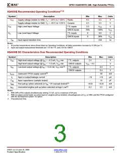
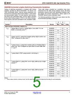
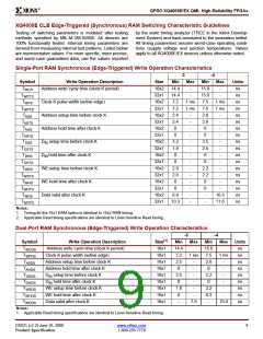
XQ4000E Switching Characteristics
XQ4000E Absolute Maximum Ratings(1)
Symbol
Description
Units
V
Supply voltage relative to GND
–0.5 to +7.0
V
CC
(2)
V
Input voltage relative to GND
–0.5 to V + 0.5
V
IN
CC
(2)
V
Voltage applied to High-Z output
Storage temperature (ambient)
–0.5 to V + 0.5
V
TS
CC
T
T
–65 to +150
+260
°C
°C
°C
°C
STG
SOL
Maximum soldering temperature (10s @ 1/16 in. = 1.5 mm)
T
Junction temperature
Ceramic package
Plastic package
+150
J
+125
Notes:
1. Stresses beyond those listed under Absolute Maximum Ratings may cause permanent damage to the device. These are stress
ratings only, and functional operation of the device at these or any other conditions beyond those listed under Operating Conditions
is not implied. Exposure to Absolute Maximum Ratings conditions for extended periods of time may affect device reliability.
2. Maximum DC excursion above V or below Ground must be limited to either 0.5V or 10 mA, whichever is easier to achieve. During
CC
transitions, the device pins may undershoot to –2.0V or overshoot to V + 2.0V, provided this over or undershoot lasts less than
CC
10 ns and with the forcing current being limited to 200 mA.
2
www.xilinx.com
DS021 (v2.2) June 25, 2000
1-800-255-7778
Product Specification

 XILINX [ XILINX, INC ]