R
Spartan-II FPGA Family: DC and Switching Characteristics
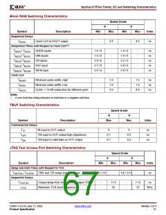
Block RAM Switching Characteristics
Speed Grade
-6
-5
Symbol
Sequential Delays
TBCKO
Description
Min
Max
Min
Max
Units
Clock CLK to DOUT output
-
3.4
-
4.0
ns
Setup/Hold Times with Respect to Clock CLK(1)
TBACK / TBCKA
BDCK/ TBCKD
BECK/ TBCKE
BRCK/ TBCKR
BWCK/ TBCKW
ADDR inputs
DIN inputs
EN inputs
1.4 / 0
1.4 / 0
2.9 / 0
2.7 / 0
2.6 / 0
-
-
-
-
-
1.4 / 0
1.4 / 0
3.2 / 0
2.9 / 0
2.8 / 0
-
-
-
-
-
ns
ns
ns
ns
ns
T
T
T
RST input
WEN input
T
Clock CLK
TBPWH
Minimum pulse width, High
-
-
-
1.9
1.9
3.0
-
-
-
1.9
1.9
4.0
ns
ns
ns
TBPWL
Minimum pulse width, Low
TBCCS
CLKA -> CLKB setup time for different ports
Notes:
1. A zero hold time listing indicates no hold time or a negative hold time.
TBUF Switching Characteristics
Speed Grade
-6
-5
Symbol
Description
Max
Max
Units
Combinatorial Delays
TIO
TOFF
TON
IN input to OUT output
0
0
ns
ns
ns
TRI input to OUT output high impedance
TRI input to valid data on OUT output
0.1
0.1
0.2
0.2
JTAG Test Access Port Switching Characteristics
Speed Grade
-6
-5
Symbol
Description
Min
Max
Min
Max
Units
Setup and Hold Times with Respect to TCK
TTAPTCK / TTCKTAP
Sequential Delays
TTCKTDO
TMS and TDI setup and hold times
4.0 / 2.0
-
4.0 / 2.0
-
ns
Output delay from clock TCK to output TDO
Maximum TCK clock frequency
-
-
11.0
33
-
-
11.0
33
ns
MHz
FTCK
DS001-3 (v2.8) June 13, 2008
Product Specification
www.xilinx.com
Module 3 of 4
67

 XILINX [ XILINX, INC ]