R
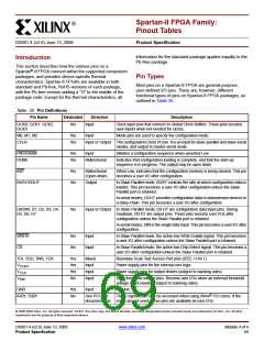
Spartan-II FPGA Family: Pinout Tables
Table 36: Spartan-II Family Package Options
(1)
Maximum Lead Pitch
Footprint
Area (mm)
Height
(mm)
Mass
(g)
Package
Leads
Type
I/O
(mm)
VQ100 / VQG100
TQ144 / TQG144
CS144 / CSG144
PQ208 / PQG208
FG256 / FGG256
FG456 / FGG456
100
144
144
208
256
456
Very Thin Quad Flat Pack (VQFP)
Thin Quad Flat Pack (TQFP)
60
0.5
16 x 16
22 x 22
1.20
1.60
1.20
3.70
2.00
2.60
0.6
1.4
0.3
5.3
0.9
2.2
92
0.5
Chip Scale Ball Grid Array (CSBGA)
Plastic Quad Flat Pack (PQFP)
Fine-pitch Ball Grid Array (FBGA)
Fine-pitch Ball Grid Array (FBGA)
92
0.8
12 x 12
140
176
284
0.5
30.6 x 30.6
17 x 17
1.0
1.0
23 x 23
Notes:
1. Package mass is 10%.
Note: Some early versions of Spartan-II devices, including
the XC2S15 and XC2S30 ES devices and the XC2S150
with date code 0045 or earlier, included a power-down pin.
For more information, see Answer Record 10500.
For additional package information, see UG112: Device
Package User Guide.
Mechanical Drawings
Detailed mechanical drawings for each package type are
available from the Xilinx web site at the specified location in
Table 38.
VCCO Banks
Some of the I/O standards require specific VCCO voltages.
These voltages are externally connected to device pins that
serve groups of IOBs, called banks. Eight I/O banks result
from separating each edge of the FPGA into two banks (see
Figure 3 in Module 2). Each bank has multiple VCCO pins
which must be connected to the same voltage. In the
smaller packages, the VCCO pins are connected between
banks, effectively reducing the number of independent
banks available (see Table 37). These interconnected
banks are shown in the Pinout Tables with VCCO pads for
multiple banks connected to the same pin.
Material Declaration Data Sheets (MDDS) are also
available on the Xilinx web site for each package.
Table 38: Xilinx Package Documentation
Package
VQ100
Drawing
MDDS
Package Drawing
PK173_VQ100
PK130_VQG100
PK169_TQ144
PK126_TQG144
PK149_CS144
PK103_CSG144
PK166_PQ208
PK123_PQG208
PK151_FG256
PK105_FGG256
PK154_FG456
PK109_FGG456
VQG100
TQ144
Package Drawing
Package Drawing
Package Drawing
Package Drawing
Package Drawing
TQG144
CS144
Table 37: Independent VCCO Banks Available
Package
VQ100
PQ208
CS144
TQ144
FG256
FG456
CSG144
PQ208
Independent Banks
1
4
8
PQG208
FG256
Package Overview
FGG256
FG456
Table 36 shows the six low-cost, space-saving production
package styles for the Spartan-II family.
Each package style is available in an environmentally
friendly lead-free (Pb-free) option. The Pb-free packages
include an extra ‘G’ in the package style name. For
example, the standard “CS144” package becomes
“CSG144” when ordered as the Pb-free option. Leaded
(non-Pb-free) packages may be available for selected
devices, with the same pin-out and without the "G" in the
ordering code; contact Xilinx sales for more information.
The mechanical dimensions of the standard and Pb-free
packages are similar, as shown in the mechanical drawings
provided in Table 38.
FGG456
DS001-4 (v2.8) June 13, 2008
Product Specification
www.xilinx.com
Module 4 of 4
70

 XILINX [ XILINX, INC ]