99
R
Spartan-II FPGA Family:
Pinout Tables
DS001-4 (v2.8) June 13, 2008
Product Specification
information for the standard package applies equally to the
Pb-free package.
Introduction
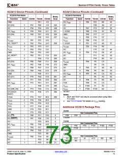
This section describes how the various pins on a
Spartan®-II FPGA connect within the supported component
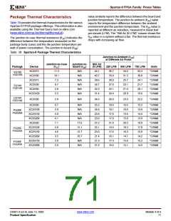
packages, and provides device-specific thermal
characteristics. Spartan-II FPGAs are available in both
standard and Pb-free, RoHS versions of each package,
with the Pb-free version adding a “G” to the middle of the
package code. Except for the thermal characteristics, all
Pin Types
Most pins on a Spartan-II FPGA are general-purpose,
user-defined I/O pins. There are, however, different
functional types of pins on Spartan-II FPGA packages, as
outlined in Table 35.
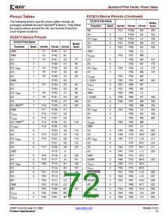
Table 35: Pin Definitions
Pin Name
Dedicated
Direction
Input
Description
GCK0, GCK1, GCK2,
GCK3
No
Clock input pins that connect to Global Clock Buffers. These pins become
user inputs when not needed for clocks.
M0, M1, M2
CCLK
Yes
Yes
Input
Mode pins are used to specify the configuration mode.
Input or Output The configuration Clock I/O pin. It is an input for slave-parallel and slave-serial
modes, and output in master-serial mode.
PROGRAM
DONE
Yes
Yes
Input
Initiates a configuration sequence when asserted Low.
Bidirectional
Indicates that configuration loading is complete, and that the start-up
sequence is in progress. The output may be open drain.
INIT
No
No
Bidirectional
(Open-drain)
When Low, indicates that the configuration memory is being cleared. This pin
becomes a user I/O after configuration.
BUSY/DOUT
Output
In Slave Parallel mode, BUSY controls the rate at which configuration data is
loaded. This pin becomes a user I/O after configuration unless the Slave
Parallel port is retained.
In serial modes, DOUT provides configuration data to downstream devices in
a daisy-chain. This pin becomes a user I/O after configuration.
D0/DIN, D1, D2, D3, D4,
D5, D6, D7
No
Input or Output In Slave Parallel mode, D0-D7 are configuration data input pins. During
readback, D0-D7 are output pins. These pins become user I/Os after
configuration unless the Slave Parallel port is retained.
In serial modes, DIN is the single data input. This pin becomes a user I/O after
configuration.
WRITE
CS
No
No
Input
Input
In Slave Parallel mode, the active-low Write Enable signal. This pin becomes
a user I/O after configuration unless the Slave Parallel port is retained.
In Slave Parallel mode, the active-low Chip Select signal. This pin becomes a
user I/O after configuration unless the Slave Parallel port is retained.
TDI, TDO, TMS, TCK
Yes
Yes
Yes
No
Mixed
Input
Input
Input
Boundary Scan Test Access Port pins (IEEE 1149.1).
Power supply pins for the internal core logic.
VCCINT
VCCO
VREF
Power supply pins for output drivers (subject to banking rules)
Input threshold voltage pins. Become user I/Os when an external threshold
voltage is not needed (subject to banking rules).
GND
Yes
No
Input
Ground.
IRDY, TRDY
See PCI core
These signals can only be accessed when using Xilinx® PCI cores. If the
documentation cores are not used, these pins are available as user I/Os.
© 2000-2008 Xilinx, Inc. All rights reserved. XILINX, the Xilinx logo, the Brand Window, and other designated brands included herein are trademarks of Xilinx, Inc. All other
trademarks are the property of their respective owners.
DS001-4 (v2.8) June 13, 2008
Product Specification
www.xilinx.com
Module 4 of 4
69

 XILINX [ XILINX, INC ]