R
Spartan-II FPGA Family: DC and Switching Characteristics
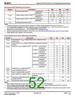
VIL
VIH
VOL
VOH
IOL
mA
IOH
mA
Input/Output
Standard
V, Min
–0.5
V, Max
V, Min
V, Max
3.6
V, Max
V, Min
CTT
AGP
VREF – 0.2
VREF – 0.2
VREF + 0.2
VREF + 0.2
VREF – 0.4
10% VCCO
VREF + 0.4
90% VCCO
8
–8
–0.5
3.6
Note (2)
Note (2)
Notes:
1.
VOL and VOH for lower drive currents are sample tested.
2. Tested according to the relevant specifications.
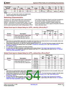
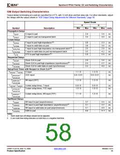
Switching Characteristics
All devices are 100% functionally tested. Internal timing
parameters are derived from measuring internal test
patterns. Listed below are representative values. For more
specific, more precise, and worst-case guaranteed data,
use the values reported by the static timing analyzer (TRCE
in the Xilinx Development System) and back-annotated to
the simulation netlist. All timing parameters assume
worst-case operating conditions (supply voltage and
junction temperature). Values apply to all Spartan-II devices
unless otherwise noted.
(1)
Global Clock Input to Output Delay for LVTTL, with DLL (Pin-to-Pin)
Speed Grade
All
-6
-5
Symbol
Description
Device
Min
Max
2.9
Max
3.3
Units
TICKOFDLL
Global clock input to output delay
using output flip-flop for LVTTL,
12 mA, fast slew rate, with DLL.
All
ns
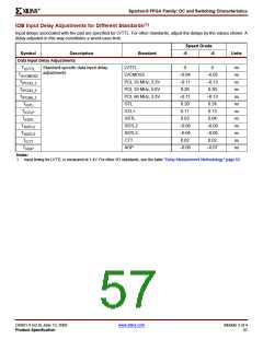
Notes:
1. Listed above are representative values where one global clock input drives one vertical clock line in each accessible column, and
where all accessible IOB and CLB flip-flops are clocked by the global clock net.
2. Output timing is measured at 1.4V with 35 pF external capacitive load for LVTTL. The 35 pF load does not apply to the Min values.
For other I/O standards and different loads, see the tables "Constants for Calculating TIOOP" and "Delay Measurement
Methodology," page 60.
3. DLL output jitter is already included in the timing calculation.
4. For data output with different standards, adjust delays with the values shown in "IOB Output Delay Adjustments for Different
Standards," page 59. For a global clock input with standards other than LVTTL, adjust delays with values from the "I/O Standard
Global Clock Input Adjustments," page 61.
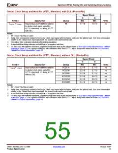
(1)
Global Clock Input to Output Delay for LVTTL, without DLL (Pin-to-Pin)
Speed Grade
All
-6
Max
4.5
4.5
4.5
4.6
4.6
4.7
-5
Max
5.4
5.4
5.4
5.5
5.5
5.6
Symbol
Description
Device
XC2S15
XC2S30
XC2S50
XC2S100
XC2S150
XC2S200
Min
Units
ns
TICKOF
Global clock input to output delay
using output flip-flop for LVTTL,
12 mA, fast slew rate, without DLL.
ns
ns
ns
ns
ns
Notes:
1. Listed above are representative values where one global clock input drives one vertical clock line in each accessible column, and
where all accessible IOB and CLB flip-flops are clocked by the global clock net.
2. Output timing is measured at 1.4V with 35 pF external capacitive load for LVTTL. The 35 pF load does not apply to the Min values.
For other I/O standards and different loads, see the tables "Constants for Calculating TIOOP" and "Delay Measurement
Methodology," page 60.
3. For data output with different standards, adjust delays with the values shown in "IOB Output Delay Adjustments for Different
Standards," page 59. For a global clock input with standards other than LVTTL, adjust delays with values from the "I/O Standard
Global Clock Input Adjustments," page 61.
DS001-3 (v2.8) June 13, 2008
Product Specification
www.xilinx.com
Module 3 of 4
54

 XILINX [ XILINX, INC ]