R
Spartan-II FPGA Family: DC and Switching Characteristics
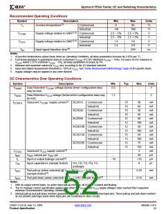
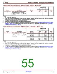
Power-On Requirements
Spartan-II FPGAs require that a minimum supply current
ICCPO be provided to the VCCINT lines for a successful
power-on. If more current is available, the FPGA can
consume more than ICCPO minimum, though this cannot
adversely affect reliability.
A maximum limit for ICCPO is not specified. Therefore the
use of foldback/crowbar supplies and fuses deserves
special attention. In these cases, limit the ICCPO current to a
level below the trip point for over-current protection in order
to avoid inadvertently shutting down the supply.
New
Old
Requirements(1) Requirements(1)
For Devices with For Devices with
Date Code 0321
or Later
Date Code
before 0321
Conditions
Device
Temperature
Grade
Junction
Symbol
Description
Temperature(2)
Min
1.50
1.00
0.25
0.50
-
Max
Min
2.00
2.00
0.50
0.50
-
Max
Units
A
(3)
ICCPO
Total VCCINT supply
current required
during power-on
–40°C≤ TJ<–20°C
–20°C ≤ TJ < 0°C
0°C ≤ TJ ≤ 85°C
85°C < TJ ≤ 100°C
–40°C≤ TJ≤ 100°C
Industrial
Industrial
Commercial
Industrial
All
-
-
-
-
A
-
-
A
-
-
A
(4,5)
TCCPO
VCCINT ramp time
50
50
ms
Notes:
1. The date code is printed on the top of the device’s package. See the "Device Part Marking" section in Module 1.
2. The expected TJ range for the design determines the ICCPO minimum requirement. Use the applicable ranges in the junction
temperature column to find the associated current values in the appropriate new or old requirements column according to the date
code. Then choose the highest of these current values to serve as the minimum ICCPO requirement that must be met. For example,
if the junction temperature for a given design is -25°C ≤ TJ ≤ 75°C, then the new minimum ICCPO requirement is 1.5A.
If 5°C ≤ TJ ≤ 90°C, then the new minimum ICCPO requirement is 0.5A.
3. The ICCPO requirement applies for a brief time (commonly only a few milliseconds) when VCCINT ramps from 0 to 2.5V.
4. The ramp time is measured from GND to VCCINT max on a fully loaded board.
5. During power-on, the VCCINT ramp must increase steadily in voltage with no dips.
6. For more information on designing to meet the power-on specifications, refer to the application note XAPP450 "Power-On Current
Requirements for the Spartan-II and Spartan-IIE Families"
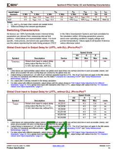
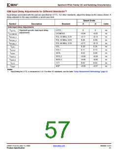
DC Input and Output Levels
Values for VIL and VIH are recommended input voltages.
Values for VOL and VOH are guaranteed output voltages
over the recommended operating conditions. Only selected
standards are tested. These are chosen to ensure that all
standards meet their specifications. The selected standards
are tested at minimum VCCO with the respective IOL and IOH
currents shown. Other standards are sample tested.
VIL
VIH
VOL
V, Max
0.4
VOH
V, Min
IOL
mA
24
IOH
mA
Input/Output
Standard
V, Min
–0.5
–0.5
–0.5
–0.5
–0.5
–0.5
–0.5
–0.5
–0.5
–0.5
–0.5
–0.5
–0.5
V, Max
0.8
V, Min
2.0
V, Max
5.5
LVTTL(1)
LVCMOS2
PCI, 3.3V
PCI, 5.0V
GTL
2.4
–24
0.7
1.7
5.5
0.4
1.9
12
–12
44% VCCINT
0.8
60% VCCINT
2.0
VCCO + 0.5
5.5
10% VCCO
0.55
90% VCCO
2.4
Note (2)
Note (2)
40
Note (2)
Note (2)
N/A
VREF – 0.05
VREF – 0.1
VREF + 0.05
VREF + 0.1
VREF + 0.1
VREF + 0.1
VREF + 0.1
VREF + 0.2
VREF + 0.2
VREF + 0.2
VREF + 0.2
3.6
0.4
N/A
GTL+
3.6
0.6
N/A
36
N/A
HSTL I
V
REF – 0.1
VREF – 0.1
REF – 0.1
VREF – 0.2
REF – 0.2
VREF – 0.2
REF – 0.2
3.6
0.4
VCCO – 0.4
VCCO – 0.4
VCCO – 0.4
VREF + 0.6
VREF + 0.8
VREF + 0.6
VREF + 0.8
8
–8
HSTL III
HSTL IV
SSTL3 I
SSTL3 II
SSTL2 I
SSTL2 II
3.6
0.4
24
–8
V
3.6
0.4
48
–8
3.6
VREF – 0.6
VREF – 0.8
VREF – 0.6
VREF – 0.8
8
–8
V
3.6
16
–16
3.6
7.6
–7.6
–15.2
V
3.6
15.2
DS001-3 (v2.8) June 13, 2008
Product Specification
www.xilinx.com
Module 3 of 4
53

 XILINX [ XILINX, INC ]