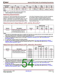
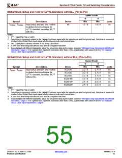
R
Spartan-II FPGA Family: DC and Switching Characteristics
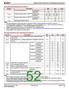
Recommended Operating Conditions
Symbol
Description
Junction temperature(1)
Min
Max
85
Units
°C
°C
V
TJ
Commercial
Industrial
0
–40
100
VCCINT
VCCO
TIN
Supply voltage relative to GND(2,5) Commercial
2.5 – 5%
2.5 – 5%
1.4
2.5 + 5%
2.5 + 5%
3.6
Industrial
V
Supply voltage relative to GND(3,5) Commercial
Industrial
Input signal transition time(4)
V
1.4
3.6
V
-
250
ns
Notes:
1. At junction temperatures above those listed as Operating Conditions, all delay parameters increase by 0.35% per °C.
2. Functional operation is guaranteed down to a minimum VCCINT of 2.25V (Nominal VCCINT – 10%). For every 50 mV reduction in
VCCINT below 2.375V (nominal VCCINT – 5%), all delay parameters increase by 3%.
3. Minimum and maximum values for VCCO vary according to the I/O standard selected.
4. Input and output measurement threshold is ~50% of VCCO. See "Delay Measurement Methodology," page 60 for specific levels.
5. Supply voltages may be applied in any order desired.
DC Characteristics Over Operating Conditions
Symbol
Description
Min
Typ
Max
Units
VDRINT
Data Retention VCCINT voltage (below which configuration data
may be lost)
2.0
-
-
V
VDRIO
Data Retention VCCO voltage (below which configuration data may
be lost)
1.2
-
-
V
ICCINTQ
Quiescent VCCINT supply current(1) XC2S15
Commercial
Industrial
-
10
10
10
10
12
12
12
12
15
15
15
15
-
30
60
mA
mA
mA
mA
mA
mA
mA
mA
mA
mA
mA
mA
mA
μA
-
XC2S30
XC2S50
Commercial
Industrial
-
30
-
60
Commercial
Industrial
-
50
-
100
50
XC2S100 Commercial
Industrial
-
-
100
50
XC2S150 Commercial
Industrial
-
-
100
75
XC2S200 Commercial
Industrial
-
-
150
2
ICCOQ
IREF
IL
Quiescent VCCO supply current(1)
VREF current per VREF pin
Input or output leakage current(2)
-
-
–10
-
-
20
-
+10
8
μA
pF
CIN
Input capacitance (sample tested)
VQ, CS, TQ, PQ, FG
packages
-
IRPU
Pad pull-up (when selected) @ VIN = 0V, VCCO = 3.3V
(sample tested)(3)
Pad pull-down (when selected) @ VIN = 3.6V (sample tested)(3)
-
-
-
-
0.25
0.15
mA
mA
IRPD
Notes:
1. With no output current loads, no active input pull-up resistors, all I/O pins 3-stated and floating.
2. The I/O leakage current specification applies only when the VCCINT and VCCO supply voltages have reached their respective
minimum Recommended Operating Conditions.
3. Internal pull-up and pull-down resistors guarantee valid logic levels at unconnected input pins. These pull-up and pull-down resistors
do not provide valid logic levels when input pins are connected to other circuits.
DS001-3 (v2.8) June 13, 2008
Product Specification
www.xilinx.com
Module 3 of 4
52

 XILINX [ XILINX, INC ]