68
R
Spartan-II FPGA Family:
DCand Switching Characteristics
DS001-3 (v2.8) June 13, 2008
Product Specification
Definition of Terms
In this document, some specifications may be designated as Advance or Preliminary. These terms are defined as follows:
Advance: Initial estimates based on simulation and/or extrapolation from other speed grades, devices, or families. Values
are subject to change. Use as estimates, not for production.
Preliminary: Based on preliminary characterization. Further changes are not expected.
Unmarked: Specifications not identified as either Advance or Preliminary are to be considered Final.
Except for pin-to-pin input and output parameters, the AC parameter delay specifications included in this document are
derived from measuring internal test patterns. All limits are representative of worst-case supply voltage and junction
temperature conditions. Typical numbers are based on measurements taken at a nominal VCCINT level of 2.5V and a junction
temperature of 25°C. The parameters included are common to popular designs and typical applications. All specifications
are subject to change without notice.
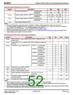
DC Specifications
(1)
Absolute Maximum Ratings
Symbol
VCCINT
VCCO
VREF
Description
Supply voltage relative to GND(2)
Supply voltage relative to GND(2)
Input reference voltage
Min
–0.5
–0.5
–0.5
–0.5
–0.5
–0.5
–0.5
–65
-
Max
3.0
Units
V
4.0
V
3.6
V
VIN
Input voltage relative to GND(3)
5V tolerant I/O(4)
No 5V tolerance(5)
5V tolerant I/O(4)
No 5V tolerance(5)
5.5
V
VCCO + 0.5
5.5
V
VTS
Voltage applied to 3-state output
V
VCCO +0.5
+150
+125
V
TSTG
TJ
Storage temperature (ambient)
Junction temperature
°C
°C
Notes:
1. Stresses beyond those listed under Absolute Maximum Ratings may cause permanent damage to the device. These are stress
ratings only, and functional operation of the device at these or any other conditions beyond those listed under Operating Conditions
is not implied. Exposure to Absolute Maximum Ratings conditions for extended periods of time may affect device reliability.
2. Power supplies may turn on in any order.
3. VIN should not exceed VCCO by more than 3.6V over extended periods of time (e.g., longer than a day).
4. Spartan®-II device I/Os are 5V Tolerant whenever the LVTTL, LVCMOS2, or PCI33_5 signal standard has been selected. With 5V
Tolerant I/Os selected, the Maximum DC overshoot must be limited to either +5.5V or 10 mA, and undershoot must be limited to
either –0.5V or 10 mA, whichever is easier to achieve. The Maximum AC conditions are as follows: The device pins may undershoot
to –2.0V or overshoot to +7.0V, provided this over/undershoot lasts no more than 11 ns with a forcing current no greater than 100 mA.
5. Without 5V Tolerant I/Os selected, the Maximum DC overshoot must be limited to either VCCO + 0.5V or 10 mA, and undershoot must
be limited to –0.5V or 10 mA, whichever is easier to achieve. The Maximum AC conditions are as follows: The device pins may
undershoot to –2.0V or overshoot to VCCO + 2.0V, provided this over/undershoot lasts no more than 11 ns with a forcing current no
greater than 100 mA.
6. For soldering guidelines, see the Packaging Information on the Xilinx® web site.
© 2000-2008 Xilinx, Inc. All rights reserved. XILINX, the Xilinx logo, the Brand Window, and other designated brands included herein are trademarks of Xilinx, Inc. All other
trademarks are the property of their respective owners.
DS001-3 (v2.8) June 13, 2008
Product Specification
www.xilinx.com
Module 3 of 4
51

 XILINX [ XILINX, INC ]