R
Spartan-II FPGA Family: Functional Description
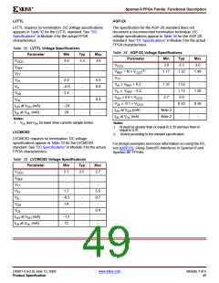
CTT
PCI33_3 and PCI66_3
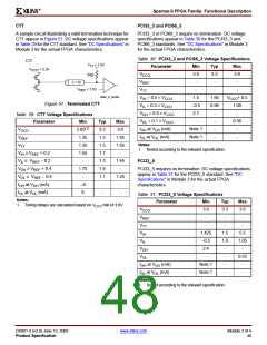
A sample circuit illustrating a valid termination technique for
CTT appear in Figure 51. DC voltage specifications appear
in Table 29 for the CTT standard. See "DC Specifications" in
Module 3 for the actual FPGA characteristics .
PCI33_3 or PCI66_3 require no termination. DC voltage
specifications appear in Table 30 for the PCI33_3 and
PCI66_3 standards. See "DC Specifications" in Module 3
for the actual FPGA characteristics.
Table 30: PCI33_3 and PCI66_3 Voltage Specifications
CTT
V
= 1.5V
TT
Parameter
Min
3.0
-
Typ
Max
V
= 3.3V
CCO
VCCO
VREF
VTT
3.3
3.6
50Ω
-
-
Z = 50
V
= 1.5V
-
-
-
REF
DS001_51_061200
V
IH = 0.5 × VCCO
1.5
–0.5
2.7
-
1.65
VCCO+ 0.5
Figure 51: Terminated CTT
Table 29: CTT Voltage Specifications
VIL = 0.3 × VCCO
0.99
1.08
V
OH = 0.9 × VCCO
OL = 0.1 × VCCO
-
-
-
-
-
V
0.36
Parameter
Min
2.05(1)
1.35
1.35
1.55
-
Typ
3.3
1.5
1.5
1.7
1.3
1.9
1.1
-
Max
I
OH at VOH (mA)
OL at VOL (mA)
Note 1
Note 1
-
-
VCCO
VREF
VTT
3.6
I
1.65
Notes:
1.65
1. Tested according to the relevant specification.
VIH ≥ VREF + 0.2
VIL ≤ VREF – 0.2
VOH ≥ VREF + 0.4
VOL ≤ VREF – 0.4
-
1.45
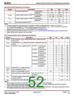
PCI33_5
1.75
-
-
PCI33_5 requires no termination. DC voltage specifications
appear in Table 31 for the PCI33_5 standard. See "DC
Specifications" in Module 3 for the actual FPGA
characteristics.
1.25
I
OH at VOH (mA)
OL at VOL (mA)
–8
-
-
I
8
-
Table 31: PCI33_5 Voltage Specifications
Notes:
1. Timing delays are calculated based on VCCO min of 3.0V.
Parameter
Min
3.0
Typ
Max
VCCO
VREF
VTT
3.3
3.6
-
-
-
-
-
-
5.5
1.05
-
VIH
1.425
–0.5
2.4
1.5
VIL
1.0
VOH
VOL
-
-
-
-
-
0.55
-
I
OH at VOH (mA)
OL at VOL (mA)
Note 1
Note 1
I
-
Notes:
1. Tested according to the relevant specification.
DS001-2 (v2.8) June 13, 2008
Product Specification
www.xilinx.com
Module 2 of 4
48

 XILINX [ XILINX, INC ]