R
Spartan-II FPGA Family: Functional Description
GTL
Table 21: GTL+ Voltage Specifications
Parameter
Min
Typ
-
Max
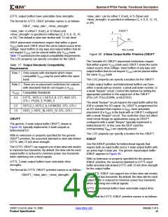
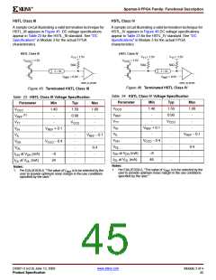
A sample circuit illustrating a valid termination technique for
GTL is shown in Figure 42. Table 20 lists DC voltage
specifications for the GTL standard. See "DC
Specifications" in Module 3 for the actual FPGA
characteristics.
VCCO
REF = N × VTT
-
0.88
1.35
0.98
-
-
1.12
1.65
-
(1)
V
1.0
1.5
1.1
0.9
-
VTT
VIH ≥ VREF + 0.1
VIL ≤ VREF – 0.1
VOH
GTL
V
= 1.2V
V
= 1.2V
TT
TT
1.02
-
50Ω
50Ω
-
V
= NA
CCO
Z = 50
VOL
0.3
-
0.45
-
0.6
-
V
= 0.8V
REF
I
I
I
OH at VOH (mA)
DS001_43_061200
OL at VOL (mA) at 0.6V
OL at VOL (mA) at 0.3V
36
-
-
-
Figure 42: Terminated GTL
Table 20: GTL Voltage Specifications
-
48
Notes:
1. N must be greater than or equal to 0.653 and less than or
equal to 0.68.
Parameter
Min
Typ
Max
VCCO
-
N/A
0.8
1.2
0.85
0.75
-
-
0.86
1.26
-
HSTL Class I
(1)
VREF = N × VTT
0.74
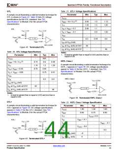
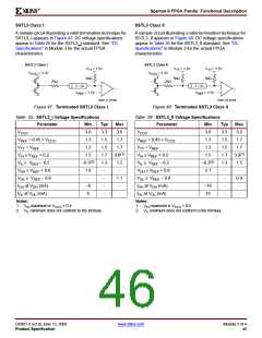
A sample circuit illustrating a valid termination technique for
HSTL_I appears in Figure 44. DC voltage specifications
appear in Table 22 for the HSTL_1 standard. See "DC
Specifications" in Module 3 for the actual FPGA
characteristics.
VTT
1.14
VIH ≥ VREF + 0.05
VIL ≤ VREF – 0.05
VOH
0.79
-
-
0.81
-
HSTL Class I
VOL
-
0.2
-
0.4
-
V
= 0.75V
TT
V
= 1.5V
I
I
I
OH at VOH (mA)
-
CCO
50Ω
OL at VOL (mA) at 0.4V
OL at VOL (mA) at 0.2V
32
-
-
-
Z = 50
-
40
V
= 0.75V
REF
Notes:
DS001_44_061200
1. N must be greater than or equal to 0.653 and less than or
equal to 0.68.
Figure 44: Terminated HSTL Class I
Table 22: HSTL Class I Voltage Specification
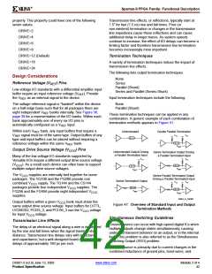
GTL+
A sample circuit illustrating a valid termination technique for
GTL+ appears in Figure 43. DC voltage specifications
appear in Table 21 for the GTL+ standard. See "DC
Specifications" in Module 3 for the actual FPGA
characteristics.
Parameter
VCCO
Min
Typ
Max
1.40
1.50
1.60
VREF
VTT
VIH
0.68
0.75
0.90
-
VCCO × 0.5
-
VREF + 0.1
-
-
-
-
-
GTL+
V
= 1.5V
V
= 1.5V
TT
TT
VIL
VREF – 0.1
50Ω
50Ω
VOH
VOL
VCCO – 0.4
-
0.4
-
V
= NA
CCO
Z = 50
V
= 1.0V
REF
I
OH at VOH (mA)
OL at VOL (mA)
–8
8
-
-
DS001_43_061200
I
-
Figure 43: Terminated GTL+
DS001-2 (v2.8) June 13, 2008
Product Specification
www.xilinx.com
Module 2 of 4
44

 XILINX [ XILINX, INC ]