R
Spartan-II FPGA Family: Functional Description
ground metallization. The IC internal ground level deviates
from the external system ground level for a short duration (a
few nanoseconds) after multiple outputs change state
simultaneously.
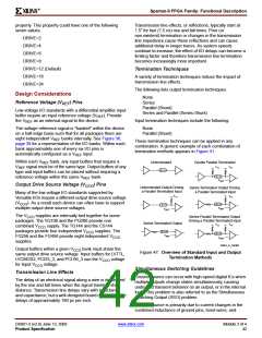
Table 18: Maximum Number of Simultaneously
Switching Outputs per Power/Ground Pair
Package
PQ,
Ground bounce affects stable Low outputs and all inputs
because they interpret the incoming signal by comparing it
to the internal ground. If the ground bounce amplitude
exceeds the actual instantaneous noise margin, then a
non-changing input can be interpreted as a short pulse with
a polarity opposite to the ground bounce.
Standard
SSTL2 Class II
CS, FG TQ, VQ
10
11
7
5
6
4
7
5
SSTL3 Class I
SSTL3 Class II
CTT
14
9
Table 18 provides the guidelines for the maximum number
of simultaneously switching outputs allowed per output
power/ground pair to avoid the effects of ground bounce.
Refer to Table 19 for the number of effective output
power/ground pairs for each Spartan-II device and package
combination.
AGP
Notes:
1. This analysis assumes a 35 pF load for each output.
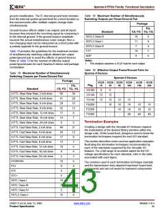
Table 19: Effective Output Power/Ground Pairs for
Table 18: Maximum Number of Simultaneously
Spartan-II Devices
Switching Outputs per Power/Ground Pair
Spartan-II Devices
Package
XC2S XC2S XC2S XC2S
XC2S
150
XC2S
200
Pkg.
15
30
50
100
PQ,
Standard
CS, FG TQ, VQ
VQ100
CS144
TQ144
PQ208
FG256
FG456
8
8
-
-
-
-
-
LVTTL Slow Slew Rate, 2 mA drive
LVTTL Slow Slew Rate, 4 mA drive
LVTTL Slow Slew Rate, 6 mA drive
LVTTL Slow Slew Rate, 8 mA drive
LVTTL Slow Slew Rate, 12 mA drive
LVTTL Slow Slew Rate, 16 mA drive
LVTTL Slow Slew Rate, 24 mA drive
LVTTL Fast Slew Rate, 2 mA drive
LVTTL Fast Slew Rate, 4 mA drive
LVTTL Fast Slew Rate, 6 mA drive
LVTTL Fast Slew Rate, 8 mA drive
LVTTL Fast Slew Rate, 12 mA drive
LVTTL Fast Slew Rate, 16 mA drive
LVTTL Fast Slew Rate, 24 mA drive
LVCMOS2
68
41
29
22
17
14
9
36
20
15
12
9
12
12
-
12
12
16
-
-
-
-
12
16
16
-
12
16
16
48
-
-
16
16
48
16
16
48
-
-
-
7
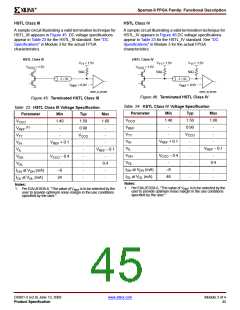
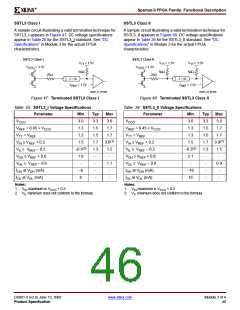
Termination Examples
5
Creating a design with the Versatile I/O features requires
the instantiation of the desired library primitive within the
design code. At the board level, designers need to know the
termination techniques required for each I/O standard.
40
24
17
13
10
8
21
12
9
This section describes some common application examples
illustrating the termination techniques recommended by
each of the standards supported by the Versatile I/O
features. For a full range of accepted values for the DC
voltage specifications for each standard, refer to the table
associated with each figure.
7
5
4
5
3
10
8
5
The resistors used in each termination technique example
and the transmission lines depicted represent board level
components and are not meant to represent components
on the device.
PCI
4
GTL
4
4
GTL+
4
4
HSTL Class I
18
9
9
HSTL Class III
5
HSTL Class IV
5
3
SSTL2 Class I
15
8
DS001-2 (v2.8) June 13, 2008
Product Specification
www.xilinx.com
Module 2 of 4
43

 XILINX [ XILINX, INC ]