R
Spartan-II FPGA Family: Functional Description
property. This property could have one of the following
seven values.
Transmission line effects, or reflections, typically start at
1.5" for fast (1.5 ns) rise and fall times. Poor (or
non-existent) termination or changes in the transmission
line impedance cause these reflections and can cause
additional delay in longer traces. As system speeds
continue to increase, the effect of I/O delays can become a
limiting factor and therefore transmission line termination
becomes increasingly more important.
DRIVE=2
DRIVE=4
DRIVE=6
DRIVE=8
DRIVE=12 (Default)
DRIVE=16
DRIVE=24
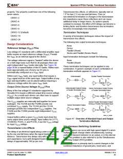
Termination Techniques
A variety of termination techniques reduce the impact of
transmission line effects.
The following lists output termination techniques:
Design Considerations
None
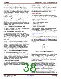
Reference Voltage (V
) Pins
Series
REF
Parallel (Shunt)
Series and Parallel (Series-Shunt)
Low-voltage I/O standards with a differential amplifier input
buffer require an input reference voltage (VREF). Provide
the VREF as an external signal to the device.
Input termination techniques include the following:
The voltage reference signal is "banked" within the device
on a half-edge basis such that for all packages there are
eight independent VREF banks internally. See Figure 36,
page 39 for a representation of the I/O banks. Within each
bank approximately one of every six I/O pins is
None
Parallel (Shunt)
These termination techniques can be applied in any
combination. A generic example of each combination of
termination methods appears in Figure 41.
automatically configured as a VREF input.
Within each VREF bank, any input buffers that require a
VREF signal must be of the same type. Output buffers of any
type and input buffers can be placed without requiring a
reference voltage within the same VREF bank.
Unterminated
Double Parallel Terminated
V
V
TT
TT
Z=50
Z=50
V
REF
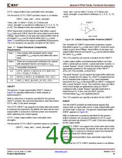
Output Drive Source Voltage (V
) Pins
CCO
Unterminated Output Driving
a Parallel Terminated Input
Series Terminated Output Driving
a Parallel Terminated Input
Many of the low voltage I/O standards supported by
Versatile I/Os require a different output drive source voltage
(VCCO). As a result each device can often have to support
multiple output drive source voltages.
V
V
TT
TT
Z=50
Z=50
V
V
REF
REF
The VCCO supplies are internally tied together for some
packages. The VQ100 and the PQ208 provide one
combined VCCO supply. The TQ144 and the CS144
packages provide four independent VCCO supplies. The
FG256 and the FG456 provide eight independent VCCO
supplies.
Series-Parallel Terminated Output
Driving a Parallel Terminated Input
Series Terminated Output
V
V
TT
TT
Z=50
Z=50
V
V
REF
REF
DS001_41_032300
Output buffers within a given VCCO bank must share the
same output drive source voltage. Input buffers for LVTTL,
LVCMOS2, PCI33_3, and PCI 66_3 use the VCCO voltage
for Input VCCO voltage.
Figure 41: Overview of Standard Input and Output
Termination Methods
Simultaneous Switching Guidelines
Transmission Line Effects
Ground bounce can occur with high-speed digital ICs when
multiple outputs change states simultaneously, causing
undesired transient behavior on an output, or in the internal
logic. This problem is also referred to as the Simultaneous
Switching Output (SSO) problem.
The delay of an electrical signal along a wire is dominated
by the rise and fall times when the signal travels a short
distance. Transmission line delays vary with inductance
and capacitance, but a well-designed board can experience
delays of approximately 180 ps per inch.
Ground bounce is primarily due to current changes in the
combined inductance of ground pins, bond wires, and
DS001-2 (v2.8) June 13, 2008
Product Specification
www.xilinx.com
Module 2 of 4
42

 XILINX [ XILINX, INC ]