R
Spartan-II FPGA Family: Functional Description
IOBUF_<slew_rate>_<drive_strength>
Versatile I/O Properties
<slew_rate> can be either F (Fast), or S (Slow) and
<drive_strength> is specified in milliamps (2, 4, 6, 8, 12, 16,
or 24).
Access to some of the Versatile I/O features (for example,
location constraints, input delay, output drive strength, and
slew rate) is available through properties associated with
these features.
Input Delay Properties
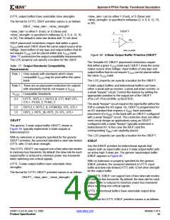
IOBUF
T
An optional delay element is associated with each IBUF.
When the IBUF drives a flip-flop within the IOB, the delay
element activates by default to ensure a zero hold-time
requirement. Use the NODELAY=TRUE property to
override this default.
I
IO
In the case when the IBUF does not drive a flip-flop within
the IOB, the delay element by default de-activates to
provide higher performance. To delay the input signal,
activate the delay element with the DELAY=TRUE property.
O
DS001_40_061200
Figure 40: Input/Output Buffer Primitiveprimitive
IOB Flip-Flop/Latch Property
(IOBUF)
The I/O Block (IOB) includes an optional register on the
input path, an optional register on the output path, and an
optional register on the 3-state control pin. The design
implementation software automatically takes advantage of
these registers when the following option for the Map
program is specified:
When the IOBUF primitive supports an I/O standard such
as LVTTL, LVCMOS, or PCI33_5, the IBUF automatically
configures as a 5V tolerant input buffer unless the VCCO for
the bank is less than 2V. If the single-ended IBUF is placed
in a bank with an HSTL standard (VCCO < 2V), the input
buffer is not 5V tolerant.
map -pr b <filename>
The voltage reference signal is "banked" within the
Spartan-II device on a half-edge basis such that for all
packages there are eight independent VREF banks
internally. See Figure 36, page 39 for a representation of
the Spartan-II FPGA I/O banks. Within each bank
approximately one of every six I/O pins is automatically
configured as a VREF input.
Alternatively, the IOB = TRUE property can be placed on a
register to force the mapper to place the register in an IOB.
Location Constraints
Specify the location of each Versatile I/O primitive with the
location constraint LOC attached to the Versatile I/O
primitive. The external port identifier indicates the value of
the location constrain. The format of the port identifier
depends on the package chosen for the specific design.
Additional restrictions on the Versatile I/O IOBUF
placement require that within a given VCCO bank each
IOBUF must share the same output source drive voltage.
Input buffers of any type and output buffers that do not
require VCCO can be placed within the same VCCO bank.
The LOC property can specify a location for the IOBUF.
The LOC properties use the following form:
LOC=A42
LOC=P37
An optional delay element is associated with the input path
in each IOBUF. When the IOBUF drives an input flip-flop
within the IOB, the delay element activates by default to
ensure a zero hold-time requirement. Override this default
with the NODELAY=TRUE property.
Output Slew Rate Property
In the case of the LVTTL output buffers (OBUF, OBUFT, and
IOBUF), slew rate control can be programmed with the
SLEW= property. By default, the slew rate for each output
buffer is reduced to minimize power bus transients when
switching non-critical signals. The SLEW= property has one
of the two following values.
In the case when the IOBUF does not drive an input flip-flop
within the IOB, the delay element de-activates by default to
provide higher performance. To delay the input signal,
activate the delay element with the DELAY=TRUE property.
SLEW=SLOW
3-state output buffers and bidirectional buffers can have
either a weak pull-up resistor, a weak pull-down resistor, or
a weak "keeper" circuit. Control this feature by adding the
appropriate primitive to the output net of the IOBUF
(PULLUP, PULLDOWN, or KEEPER).
SLEW=FAST
Output Drive Strength Property
For the LVTTL output buffers (OBUF, OBUFT, and IOBUF,
the desired drive strength can be specified with the DRIVE=
DS001-2 (v2.8) June 13, 2008
Product Specification
www.xilinx.com
Module 2 of 4
41

 XILINX [ XILINX, INC ]