R
Spartan-II FPGA Family: Functional Description
or one of the global clock input buffers (IBUFG) on the same
edge of the device (top or bottom) must source this clock
signal.
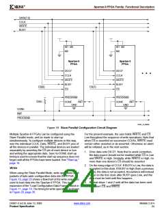
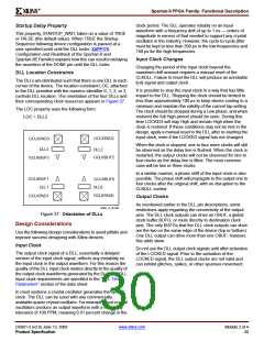
BUFGDLL Pin Descriptions
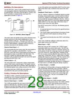
Use the BUFGDLL macro as the simplest way to provide
zero propagation delay for a high-fanout on-chip clock from
an external input. This macro uses the IBUFG, CLKDLL and
BUFG primitives to implement the most basic DLL
application as shown in Figure 25.
Feedback Clock Input — CLKFB
The DLL requires a reference or feedback signal to provide
the delay-compensated output. Connect only the CLK0 or
CLK2X DLL outputs to the feedback clock input (CLKFB)
pin to provide the necessary feedback to the DLL. Either a
global clock buffer (BUFG) or one of the global clock input
buffers (IBUFG) on the same edge of the device (top or
bottom) must source this clock signal.
IBUFG
BUFG
CLKDLL
I
O
O
I
CLKIN
CLK0
CLK90
CLK180
CLK270
CLKFB
If an IBUFG sources the CLKFB pin, the following special
rules apply.
CLK2X
CLKDV
RST
1. An external input port must source the signal that drives
the IBUFG I pin.
LOCKED
2. The CLK2X output must feed back to the device if both
the CLK0 and CLK2X outputs are driving off chip
devices.
DS001_25_032300
Figure 25: BUFGDLL Block Diagram
3. That signal must directly drive only OBUFs and nothing
else.
This macro does not provide access to the advanced clock
domain controls or to the clock multiplication or clock
division features of the DLL. This macro also does not
provide access to the RST or LOCKED pins of the DLL. For
access to these features, a designer must use the DLL
primitives described in the following sections.
These rules enable the software to determine which DLL
clock output sources the CLKFB pin.
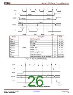
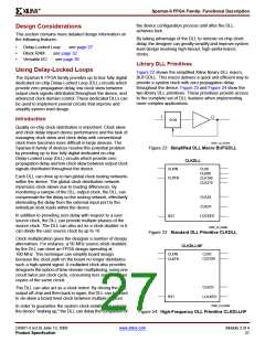
Reset Input — RST
When the reset pin RST activates, the LOCKED signal
deactivates within four source clock cycles. The RST pin,
active High, must either connect to a dynamic signal or be
tied to ground. As the DLL delay taps reset to zero, glitches
can occur on the DLL clock output pins. Activation of the
RST pin can also severely affect the duty cycle of the clock
output pins. Furthermore, the DLL output clocks no longer
deskew with respect to one another. The DLL must be reset
when the input clock frequency changes, if the device is
reconfigured in Boundary-Scan mode, if the device
Source Clock Input — I
The I pin provides the user source clock, the clock signal on
which the DLL operates, to the BUFGDLL. For the
BUFGDLL macro the source clock frequency must fall in the
low frequency range as specified in the data sheet. The
BUFGDLL requires an external signal source clock.
Therefore, only an external input port can source the signal
that drives the BUFGDLL I pin.
Clock Output — O
undergoes a hot swap, and after the device is configured if
the input clock is not stable during the startup sequence.
The clock output pin O represents a delay-compensated
version of the source clock (I) signal. This signal, sourced
by a global clock buffer BUFG primitive, takes advantage of
the dedicated global clock routing resources of the device.
2x Clock Output — CLK2X
The output pin CLK2X provides a frequency-doubled clock
with an automatic 50/50 duty-cycle correction. Until the
CLKDLL has achieved lock, the CLK2X output appears as a
1x version of the input clock with a 25/75 duty cycle. This
behavior allows the DLL to lock on the correct edge with
respect to source clock. This pin is not available on the
CLKDLLHF primitive.
The output clock has a 50/50 duty cycle unless you
deactivate the duty cycle correction property.
CLKDLL Primitive Pin Descriptions
The library CLKDLL primitives provide access to the
complete set of DLL features needed when implementing
more complex applications with the DLL.
Clock Divide Output — CLKDV
The clock divide output pin CLKDV provides a lower
frequency version of the source clock. The CLKDV_DIVIDE
property controls CLKDV such that the source clock is
divided by N where N is either 1.5, 2, 2.5, 3, 4, 5, 8, or 16.
Source Clock Input — CLKIN
The CLKIN pin provides the user source clock (the clock
signal on which the DLL operates) to the DLL. The CLKIN
frequency must fall in the ranges specified in the data sheet.
A global clock buffer (BUFG) driven from another CLKDLL
This feature provides automatic duty cycle correction. The
CLKDV output pin has a 50/50 duty cycle for all values of the
DS001-2 (v2.8) June 13, 2008
Product Specification
www.xilinx.com
Module 2 of 4
28

 XILINX [ XILINX, INC ]