R
Spartan-II FPGA Family: Functional Description
If other clock output is needed, the clock could access a
BUFG only if the DLLs are constrained to exist on opposite
edges (Top or Bottom) of the device.
Useful Application Examples
The Spartan-II FPGA DLL can be used in a variety of
creative and useful applications. The following examples
show some of the more common applications.
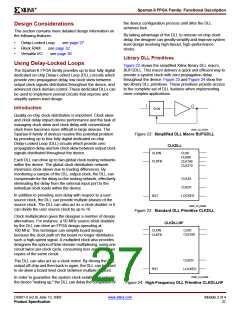
CLKDLL
Standard Usage
IBUFG
CLKIN
CLKFB
CLK0
CLK90
CLK180
CLK270
The circuit shown in Figure 28 resembles the BUFGDLL
macro implemented to provide access to the RST and
LOCKED pins of the CLKDLL.
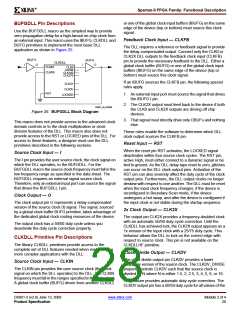
BUFG
IBUFG
CLK2X
CLKDV
CLKDLL
BUFG
CLKIN
CLKFB
CLK0
INV
CLK90
CLK180
CLK270
SRL16
RST
D
Q
LOCKED
WCLK
CLK2X
CLKDV
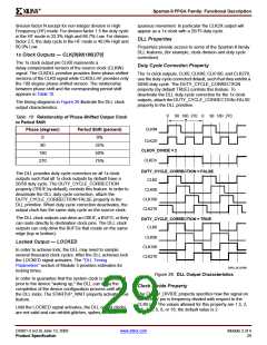
IBUF
OBUF
A3
CLKDLL
RST
LOCKED
A2
A1
A0
CLKIN
CLKFB
CLK0
CLK90
CLK180
CLK270
DS001_28_061200
Figure 28: Standard DLL Implementation
BUFG
CLK2X
CLKDV
Deskew of Clock and Its 2x Multiple
OBUF
The circuit shown in Figure 29 implements a 2x clock
multiplier and also uses the CLK0 clock output with zero ns
skew between registers on the same chip. A clock divider
circuit could alternatively be implemented using similar
connections.
RST
LOCKED
DS001_30_061200
IBUFG
CLKDLL
BUFG
Figure 30: DLL Generation of 4x Clock
CLKIN
CLKFB
CLK0
CLK90
CLK180
CLK270
When using this circuit it is vital to use the SRL16 cell to
reset the second DLL after the initial chip reset. If this is not
done, the second DLL may not recognize the change of
frequencies from when the input changes from a 1x (25/75)
waveform to a 2x (50/50) waveform. It is not recommended
to cascade more than two DLLs.
BUFG
OBUF
CLK2X
CLKDV
IBUF
RST
LOCKED
For design examples and more information on using the
DLL, see XAPP174, Using Delay-Locked Loops in Spartan-II
FPGAs.
DS001_29_061200
Figure 29: DLL Deskew of Clock and 2x Multiple
Because any single DLL can only access at most two
BUFGs, any additional output clock signals must be routed
from the DLL in this example on the high speed backbone
routing.
Generating a 4x Clock
By connecting two DLL circuits each implementing a 2x
clock multiplier in series as shown in Figure 30, a 4x clock
multiply can be implemented with zero skew between
registers in the same device.
DS001-2 (v2.8) June 13, 2008
Product Specification
www.xilinx.com
Module 2 of 4
31

 XILINX [ XILINX, INC ]