R
Spartan-II FPGA Family: Functional Description
clock period. The DLL operates reliably on an input
waveform with a frequency drift of up to 1 ns — orders of
magnitude in excess of that needed to support any crystal
oscillator in the industry. However, the cycle-to-cycle jitter
must be kept to less than 300 ps in the low frequencies and
150 ps for the high frequencies.
Startup Delay Property
This property, STARTUP_WAIT, takes on a value of TRUE
or FALSE (the default value). When TRUE the Startup
Sequence following device configuration is paused at a
user-specified point until the DLL locks. XAPP176:
Configuration and Readback of the Spartan-II and
Spartan-IIE Families explains how this can result in delaying
the assertion of the DONE pin until the DLL locks.
Input Clock Changes
Changing the period of the input clock beyond the
maximum drift amount requires a manual reset of the
CLKDLL. Failure to reset the DLL will produce an unreliable
lock signal and output clock.
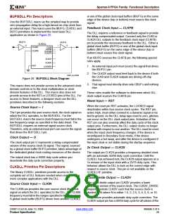
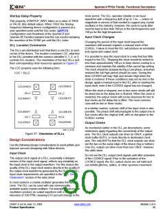
DLL Location Constraints
The DLLs are distributed such that there is one DLL in each
corner of the device. The location constraint LOC, attached
to the DLL primitive with the numeric identifier 0, 1, 2, or 3,
controls DLL location. The orientation of the four DLLs and
their corresponding clock resources appears in Figure 27.
It is possible to stop the input clock in a way that has little
impact to the DLL. Stopping the clock should be limited to
less than approximately 100 μs to keep device cooling to a
minimum and maintain the validity of the current tap setting.
The clock should be stopped during a Low phase, and when
restored the full High period should be seen. During this
time LOCKED will stay High and remain High when the
clock is restored. If these conditions may not be met in the
design, apply a manual reset to the DLL after re-starting the
input clock, even if the LOCKED signal has not changed.
The LOC property uses the following form.
LOC = DLL2
GCLKPAD2
GCLKPAD3
When the clock is stopped, one to four more clocks will still
be observed as the delay line is flushed. When the clock is
restarted, the output clocks will not be observed for one to
four clocks as the delay line is filled. The most common
case will be two or three clocks.
DLL3
DLL2
GCLKBUF2
GCLKBUF3
In a similar manner, a phase shift of the input clock is also
possible. The phase shift will propagate to the output one to
four clocks after the original shift, with no disruption to the
CLKDLL control.
GCLKBUF1
DLL1
GCLKBUF0
DLL0
GCLKPAD0
GCLKPAD1
Output Clocks
As mentioned earlier in the DLL pin descriptions, some
restrictions apply regarding the connectivity of the output
pins. The DLL clock outputs can drive an OBUF, a global
clock buffer BUFG, or route directly to destination clock
pins. The only BUFGs that the DLL clock outputs can drive
are the two on the same edge of the device (top or bottom).
One DLL output can drive more than one OBUF; however,
this adds skew.
DS001_27_061308
Figure 27: Orientation of DLLs
Design Considerations
Use the following design considerations to avoid pitfalls and
improve success designing with Xilinx devices.
Input Clock
Do not use the DLL output clock signals until after activation
of the LOCKED signal. Prior to the activation of the
LOCKED signal, the DLL output clocks are not valid and
can exhibit glitches, spikes, or other spurious movement.
The output clock signal of a DLL, essentially a delayed
version of the input clock signal, reflects any instability on
the input clock in the output waveform. For this reason the
quality of the DLL input clock relates directly to the quality of
the output clock waveforms generated by the DLL. The DLL
input clock requirements are specified in the "DLL Timing
Parameters" section of the data sheet.
In most systems a crystal oscillator generates the system
clock. The DLL can be used with any commercially
available quartz crystal oscillator. For example, most crystal
oscillators produce an output waveform with a frequency
tolerance of 100 PPM, meaning 0.01 percent change in the
DS001-2 (v2.8) June 13, 2008
Product Specification
www.xilinx.com
Module 2 of 4
30

 XILINX [ XILINX, INC ]