R
Spartan-II FPGA Family: Functional Description
the configuration data are being loaded, the CCLK
frequency is always 2.5 MHz. This frequency is used until
the ConfigRate bits, part of the configuration file, have been
loaded into the FPGA, at which point, the frequency
changes to the selected ConfigRate. Unless a different
frequency is specified in the design, the default ConfigRate
is 4 MHz. The frequency of the CCLK signal created by the
internal oscillator has a variance of +45%, –30% from the
specified value.
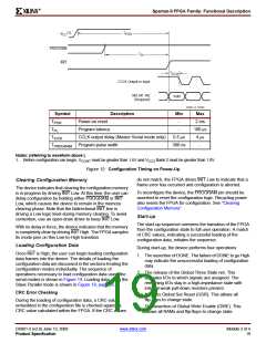
Master Serial Mode
In Master Serial mode, the CCLK output of the FPGA drives
a Xilinx PROM which feeds a serial stream of configuration
data to the FPGA’s DIN input. Figure 15 shows a Master
Serial FPGA configuring a Slave Serial FPGA from a
PROM. A Spartan-II device in Master Serial mode should
be connected as shown for the device on the left side.
Master Serial mode is selected by a <00x> on the mode
pins (M0, M1, M2). The PROM RESET pin is driven by INIT,
and CE input is driven by DONE. The interface is identical
to the slave serial mode except that an oscillator internal to
the FPGA is used to generate the configuration clock
(CCLK). Any of a number of different frequencies ranging
from 4 to 60 MHz can be set using the ConfigRate option in
the Xilinx software. On power-up, while the first 60 bytes of
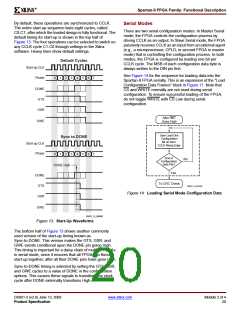
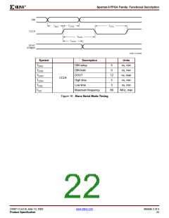
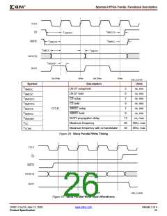
Figure 17 shows the timing for Master Serial configuration.
The FPGA accepts one bit of configuration data on each
rising CCLK edge. After the FPGA has been loaded, the
data for the next device in a daisy-chain is presented on the
DOUT pin after the rising CCLK edge.
CCLK
(Output)
T
CKDS
T
DSCK
Serial Data In
T
CCO
Serial DOUT
(Output)
DS001_17_110101
.
Symbol
TDSCK
Description
Units
ns, min
ns, min
-
DIN setup
DIN hold
5.0
0.0
TCKDS
CCLK
Frequency tolerance with respect to
nominal
+45%, –30%
Figure 17: Master Serial Mode Timing
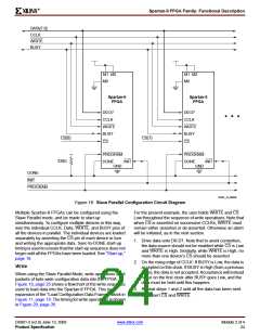
The agent controlling configuration is not shown. Typically,
a processor, a microcontroller, or CPLD controls the Slave
Parallel interface. The controlling agent provides byte-wide
configuration data, CCLK, a Chip Select (CS) signal and a
Write signal (WRITE). If BUSY is asserted (High) by the
FPGA, the data must be held until BUSY goes Low.
Slave Parallel Mode
The Slave Parallel mode is the fastest configuration option.
Byte-wide data is written into the FPGA. A BUSY flag is
provided for controlling the flow of data at a clock frequency
FCCNH above 50 MHz.
Figure 18, page 24 shows the connections for two
Spartan-II devices using the Slave Parallel mode. Slave
Parallel mode is selected by a <011> on the mode pins (M0,
M1, M2).
After configuration, the pins of the Slave Parallel port
(D0-D7) can be used as additional user I/O. Alternatively,
the port may be retained to permit high-speed 8-bit
readback. Then data can be read by de-asserting WRITE.
See "Readback," page 25.
If a configuration file of the format .bit, .rbt, or non-swapped
HEX is used for parallel programming, then the most
significant bit (i.e. the left-most bit of each configuration
byte, as displayed in a text editor) must be routed to the D0
input on the FPGA.
DS001-2 (v2.8) June 13, 2008
Product Specification
www.xilinx.com
Module 2 of 4
23

 XILINX [ XILINX, INC ]