R
Spartan-II FPGA Family: Functional Description
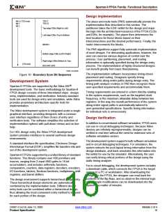
By default, these operations are synchronized to CCLK.
The entire start-up sequence lasts eight cycles, called
C0-C7, after which the loaded design is fully functional. The
default timing for start-up is shown in the top half of
Figure 13. The four operations can be selected to switch on
any CCLK cycle C1-C6 through settings in the Xilinx
software. Heavy lines show default settings.
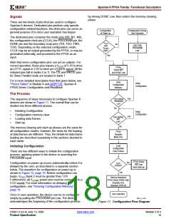
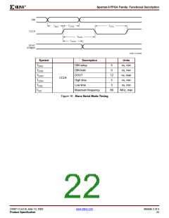
Serial Modes
There are two serial configuration modes: In Master Serial
mode, the FPGA controls the configuration process by
driving CCLK as an output. In Slave Serial mode, the FPGA
passively receives CCLK as an input from an external agent
(e.g., a microprocessor, CPLD, or second FPGA in master
mode) that is controlling the configuration process. In both
modes, the FPGA is configured by loading one bit per
CCLK cycle. The MSB of each configuration data byte is
always written to the DIN pin first.
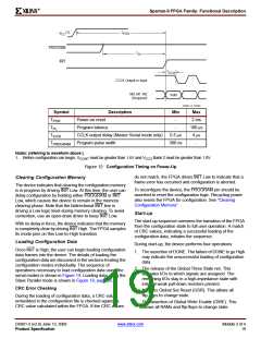
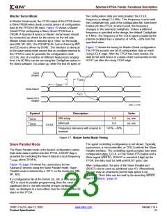
Default Cycles
Start-up CLK
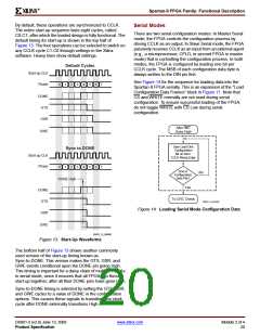
See Figure 14 for the sequence for loading data into the
Spartan-II FPGA serially. This is an expansion of the "Load
Configuration Data Frames" block in Figure 11. Note that
CS and WRITE normally are not used during serial
configuration. To ensure successful loading of the FPGA,
do not toggle WRITE with CS Low during serial
configuration.
Phase
0
1
2
3
4
5
6 7
DONE
GTS
GSR
After INIT
Goes High
GWE
User Load One
Configuration
Sync to DONE
Bit on Next
CCLK Rising Edge
Start-up CLK
Phase
0
1
2
3
4
5
6 7
End of
No
Configuration
Data File?
DONE High
Yes
DONE
GTS
To CRC Check
DS001_14_042403
Figure 14: Loading Serial Mode Configuration Data
GSR
GWE
DS001_13_090600
Figure 13: Start-Up Waveforms
The bottom half of Figure 13 shows another commonly
used version of the start-up timing known as
Sync-to-DONE. This version makes the GTS, GSR, and
GWE events conditional upon the DONE pin going High.
This timing is important for a daisy chain of multiple FPGAs
in serial mode, since it ensures that all FPGAs go through
start-up together, after all their DONE pins have gone High.
Sync-to-DONE timing is selected by setting the GTS, GSR,
and GWE cycles to a value of DONE in the configuration
options. This causes these signals to transition one clock
cycle after DONE externally transitions High.
DS001-2 (v2.8) June 13, 2008
Product Specification
www.xilinx.com
Module 2 of 4
20

 XILINX [ XILINX, INC ]