R
Spartan-II FPGA Family: Functional Description
(1)
T
V
POR
CC
PROGRAM
INIT
T
PL
T
ICCK
Valid
CCLK Output or Input
M0, M1, M2
(Required)
DS001_12_102301
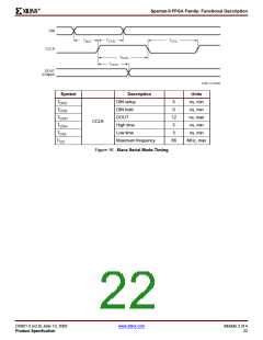
.
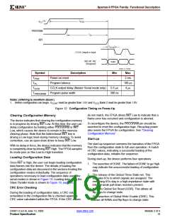
Symbol
TPOR
Description
Min
Max
Power-on reset
Program latency
-
2 ms
100 μs
4 μs
-
TPL
-
TICCK
CCLK output delay (Master Serial mode only)
Program pulse width
0.5 μs
300 ns
TPROGRAM
Notes: (referring to waveform above:)
1. Before configuration can begin, VCCINT must be greater than 1.6V and VCCO Bank 2 must be greater than 1.0V.
Figure 12: Configuration Timing on Power-Up
do not match, the FPGA drives INIT Low to indicate that a
frame error has occurred and configuration is aborted.
Clearing Configuration Memory
The device indicates that clearing the configuration memory
is in progress by driving INIT Low. At this time, the user can
delay configuration by holding either PROGRAM or INIT
Low, which causes the device to remain in the memory
clearing phase. Note that the bidirectional INIT line is
driving a Low logic level during memory clearing. To avoid
contention, use an open-drain driver to keep INIT Low.
To reconfigure the device, the PROGRAM pin should be
asserted to reset the configuration logic. Recycling power
also resets the FPGA for configuration. See "Clearing
Configuration Memory".
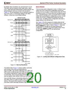
Start-up
The start-up sequence oversees the transition of the FPGA
from the configuration state to full user operation. A match
of CRC values, indicating a successful loading of the
configuration data, initiates the sequence.
With no delay in force, the device indicates that the memory
is completely clear by driving INIT High. The FPGA samples
its mode pins on this Low-to-High transition.
Loading Configuration Data
During start-up, the device performs four operations:
Once INIT is High, the user can begin loading configuration
data frames into the device. The details of loading the
configuration data are discussed in the sections treating the
configuration modes individually. The sequence of
operations necessary to load configuration data using the
serial modes is shown in Figure 14. Loading data using the
Slave Parallel mode is shown in Figure 19, page 25.
1. The assertion of DONE. The failure of DONE to go High
may indicate the unsuccessful loading of configuration
data.
2. The release of the Global Three State net. This
activates I/Os to which signals are assigned. The
remaining I/Os stay in a high-impedance state with
internal weak pull-down resistors present.
CRC Error Checking
3. Negates Global Set Reset (GSR). This allows all
flip-flops to change state.
During the loading of configuration data, a CRC value
embedded in the configuration file is checked against a
CRC value calculated within the FPGA. If the CRC values
4. The assertion of Global Write Enable (GWE). This
allows all RAMs and flip-flops to change state.
DS001-2 (v2.8) June 13, 2008
Product Specification
www.xilinx.com
Module 2 of 4
19

 XILINX [ XILINX, INC ]