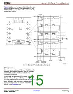
R
Spartan-II FPGA Family: Functional Description
by driving DONE Low, then enters the memory-clearing
phase.
Signals
There are two kinds of pins that are used to configure
Spartan-II devices: Dedicated pins perform only specific
configuration-related functions; the other pins can serve as
general purpose I/Os once user operation has begun.
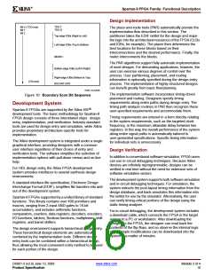
Configuration
at Power-up
Configuration During
User Operation
The dedicated pins comprise the mode pins (M2, M1, M0),
the configuration clock pin (CCLK), the PROGRAM pin, the
DONE pin and the boundary-scan pins (TDI, TDO, TMS,
TCK). Depending on the selected configuration mode,
CCLK may be an output generated by the FPGA, or may be
generated externally, and provided to the FPGA as an
input.
VCCO
AND
VCCINT
High?
No
User Pulls
PROGRAM
Low
Yes
Note that some configuration pins can act as outputs. For
correct operation, these pins require a VCCO of 3.3V to drive
an LVTTL signal or 2.5V to drive an LVCMOS signal. All the
relevant pins fall in banks 2 or 3. The CS and WRITE pins
for Slave Parallel mode are located in bank 1.
FPGA
Drives INIT
and DONE Low
For a more detailed description than that given below, see
"Pinout Tables" in Module 4 and XAPP176, Spartan-II
FPGA Series Configuration and Readback.
Clear
Configuration
Memory
Delay
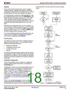
Configuration
The Process
Yes
User Holding
PROGRAM
Low?
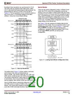
The sequence of steps necessary to configure Spartan-II
devices are shown in Figure 11. The overall flow can be
divided into three different phases.
No
•
•
•
•
Initiating Configuration
Configuration memory clear
Loading data frames
Start-up
Delay
Configuration
Yes
User Holding
INIT
Low?
No
The memory clearing and start-up phases are the same for
all configuration modes; however, the steps for the loading
of data frames are different. Thus, the details for data frame
loading are described separately in the sections devoted to
each mode.
FPGA
Samples
Mode Pins
Load
Configuration
Data Frames
Initiating Configuration
There are two different ways to initiate the configuration
process: applying power to the device or asserting the
PROGRAM input.
FPGA Drives
INIT Low
Abort Start-up
No
Configuration on power-up occurs automatically unless it is
delayed by the user, as described in a separate section
below. The waveform for configuration on power-up is
shown in Figure 12, page 19. Before configuration can
begin, VCCO Bank 2 must be greater than 1.0V.
Furthermore, all VCCINT power pins must be connected to a
2.5V supply. For more information on delaying
configuration, see "Clearing Configuration Memory,"
page 19.
CRC
Correct?
Yes
Start-up Sequence
FPGA Drives DONE High,
Activates I/Os,
Releases GSR net
User Operation
Once in user operation, the device can be re-configured
simply by pulling the PROGRAM pin Low. The device
acknowledges the beginning of the configuration process
DS001_11_111501
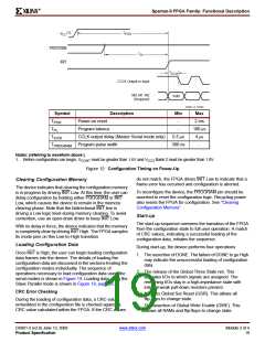
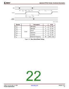
Figure 11: Configuration Flow Diagram
DS001-2 (v2.8) June 13, 2008
Product Specification
www.xilinx.com
Module 2 of 4
18

 XILINX [ XILINX, INC ]