R
Spartan-II FPGA Family: Functional Description
Design Implementation
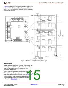
TDO.T
TDO.O
Bit 0 ( TDO end)
Bit 1
Bit 2
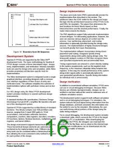
The place-and-route tools (PAR) automatically provide the
implementation flow described in this section. The
partitioner takes the EDIF netlist for the design and maps
the logic into the architectural resources of the FPGA (CLBs
and IOBs, for example). The placer then determines the
best locations for these blocks based on their
Top-edge IOBs (Right to Left)
Left-edge IOBs (Top to Bottom)
interconnections and the desired performance. Finally, the
router interconnects the blocks.
MODE.I
The PAR algorithms support fully automatic implementation
of most designs. For demanding applications, however, the
user can exercise various degrees of control over the
process. User partitioning, placement, and routing
information is optionally specified during the design-entry
process. The implementation of highly structured designs
can benefit greatly from basic floorplanning.
Bottom-edge IOBs (Left to Right)
Right-edge IOBs (Bottom to Top)
BSCANT.UPD
(TDI end)
DS001_10_032300
The implementation software incorporates timing-driven
placement and routing. Designers specify timing
Figure 10: Boundary Scan Bit Sequence
requirements along entire paths during design entry. The
timing path analysis routines in PAR then recognize these
user-specified requirements and accommodate them.
Development System
Spartan-II FPGAs are supported by the Xilinx ISE®
development tools. The basic methodology for Spartan-II
FPGA design consists of three interrelated steps: design
entry, implementation, and verification. Industry-standard
tools are used for design entry and simulation, while Xilinx
provides proprietary architecture-specific tools for
implementation.
Timing requirements are entered in a form directly relating
to the system requirements, such as the targeted clock
frequency, or the maximum allowable delay between two
registers. In this way, the overall performance of the system
along entire signal paths is automatically tailored to
user-generated specifications. Specific timing information
for individual nets is unnecessary.
The Xilinx development system is integrated under a single
graphical interface, providing designers with a common
user interface regardless of their choice of entry and
verification tools. The software simplifies the selection of
implementation options with pull-down menus and on-line
help.
Design Verification
In addition to conventional software simulation, FPGA users
can use in-circuit debugging techniques. Because Xilinx
devices are infinitely reprogrammable, designs can be
verified in real time without the need for extensive sets of
software simulation vectors.
For HDL design entry, the Xilinx FPGA development
system provides interfaces to several synthesis design
environments.
The development system supports both software simulation
and in-circuit debugging techniques. For simulation, the
system extracts the post-layout timing information from the
design database, and back-annotates this information into
the netlist for use by the simulator. Alternatively, the user
can verify timing-critical portions of the design using the
static timing analyzer.
A standard interface-file specification, Electronic Design
Interchange Format (EDIF), simplifies file transfers into and
out of the development system.
Spartan-II FPGAs supported by a unified library of standard
functions. This library contains over 400 primitives and
macros, ranging from 2-input AND gates to 16-bit
accumulators, and includes arithmetic functions,
comparators, counters, data registers, decoders, encoders,
I/O functions, latches, Boolean functions, multiplexers, shift
registers, and barrel shifters.
For in-circuit debugging, the development system includes
a download cable, which connects the FPGA in the target
system to a PC or workstation. After downloading the
design into the FPGA, the designer can read back the
contents of the flip-flops, and so observe the internal logic
state. Simple modifications can be downloaded into the
system in a matter of minutes.
The design environment supports hierarchical design entry.
These hierarchical design elements are automatically
combined by the implementation tools. Different design
entry tools can be combined within a hierarchical design,
thus allowing the most convenient entry method to be used
for each portion of the design.
DS001-2 (v2.8) June 13, 2008
Product Specification
www.xilinx.com
Module 2 of 4
16

 XILINX [ XILINX, INC ]