R
Spartan-II FPGA Family: Functional Description
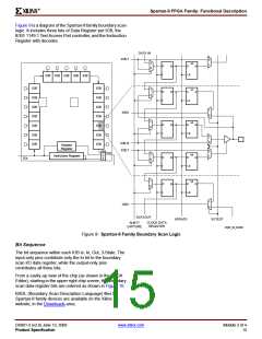
Figure 9 is a diagram of the Spartan-II family boundary scan
logic. It includes three bits of Data Register per IOB, the
IEEE 1149.1 Test Access Port controller, and the Instruction
Register with decodes.
DATA IN
IOB.T
0
1
sd
1
D
D
Q
Q
D
Q
0
LE
IOB IOB IOB IOB IOB
IOB
IOB
IOB
IOB
IOB
IOB
IOB
IOB
IOB
IOB
IOB
IOB
IOB
IOB
sd
1
0
D
Q
LE
1
0
IOB.I
1
sd
D
Q
D
Q
0
LE
1
0
IOB.Q
IOB.T
Bypass
Register
0
1
M
U
X
TDO
1
sd
Instruction Register
D
Q
D
Q
TDI
0
LE
1
sd
D
Q
D
Q
0
LE
1
0
IOB.I
DATAOUT
UPDATE
EXTEST
CLOCK DATA
REGISTER
SHIFT/
CAPTURE
DS001_09_032300
Figure 9: Spartan-II Family Boundary Scan Logic
Bit Sequence
The bit sequence within each IOB is: In, Out, 3-State. The
input-only pins contribute only the In bit to the boundary
scan I/O data register, while the output-only pins
contributes all three bits.
From a cavity-up view of the chip (as shown in the FPGA
Editor), starting in the upper right chip corner, the boundary
scan data-register bits are ordered as shown in Figure 10.
BSDL (Boundary Scan Description Language) files for
Spartan-II family devices are available on the Xilinx
website, in the Downloads area.
DS001-2 (v2.8) June 13, 2008
Product Specification
www.xilinx.com
Module 2 of 4
15

 XILINX [ XILINX, INC ]