R
XCR3064A: 64 Macrocell CPLD With Enhanced Clocking
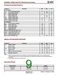
Programming Specifications
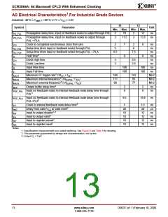
Symbol
Parameter
Min.
3.0
Max.
Unit
DC Parameters
V
V
supply program/verify
CC
3.6
V
mA
V
CCP
I
I
limit program/verify
200
CCP
CC
V
V
V
V
Input Voltage (High)
Input Voltage (Low)
Output Voltage (Low)
Output Voltage (High)
Output current (Low)
Output current (High)
2.0
IH
0.8
0.5
V
IL
V
SOL
SOH
2.4
8
V
TDO_I
TDO_I
mA
mA
OL
8
OH
AC Parameters
f
TCK maximum frequency
Pulse width erase
10
100
10
MHz
ms
ms
µs
µs
ns
MAX
PWE
PWP
PWV
INIT
Pulse width program
Pulse width verify
10
Initialization time
100
10
TMS_SU TMS setup time before TCK ↑
TDI_SU
TMS_H
TDI_H
TDI setup time before TCK ↑
TMS hold time after TCK ↑
TDI hold time after TCK ↑
10
ns
25
ns
25
ns
TDO_CO TDO valid after TCK ↓
40
ns
ABSOLUTE MAXIMUM RATINGS1
Symbol
Parameter
Min.
-0.5
Max.
4.6
Unit
V
2
Supply Voltage
Input Voltage
Output Voltage
Input current
V
CC
I
-1.2
-0.5
-30
-40
-65
5.75
V
V
V
V
V
+0.5
CC
OUT
30
mA
°C
°C
I
IN
Maximum junction temperature
Storage temperature
150
150
T
T
J
str
Notes:
1. Stresses above those listed may cause malfunction or permanent damage to the device. This is a stress rating only.
Functional operation at these or any other condition above those indicated in the operational and programming specification
is not implied.
2. The chip supply voltage must rise monotonically.
Operating Range
Product Grade
Commercial
Industrial
Temperature
0 to +70°C
Voltage
3.0 to 3.6V
2.7 to 3.6V
-40 to +85°C
9
www.xilinx.com
DS037 (v1.1) February 10, 2000
1-800-255-7778

 XILINX [ XILINX, INC ]