R
XCR3064A: 64 Macrocell CPLD With Enhanced Clocking
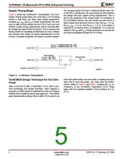
45
TYPICAL
40
35
30
25
I
CC
(mA)
20
15
10
5
0
1
20
40
60
80
100
120
140
FREQUENCY (MHz)
SP00700
Figure 5:
I
vs. Frequency at V = 3.3 V, 25°C
CC CC
Table 1: I vs. Frequency (V = 3.3 V, 25°C)
CC
CC
Frequency (MHz)
0
1
20
40
60
14.0
80
100
23.2
120
140
Typical I (mA)
0.03
0.3
4.7
9.4
18.7
27.7
32.4
CC
resistor to keep the JTAG signs from floating when they are
not being used.
JTAG Testing Capability
JTAG is the commonly-used acronym for the Boundary
Scan Test (BST) feature defined for integrated circuits by
IEEE Standard 1149.1. This standard defines input/output
pins, logic control functions, and commands which facilitate
both board and device level testing without the use of spe-
cialized test equipment. The Xilinx XCR3064A devices use
the JTAG interface for In-System Programming/Repro-
gramming. Although only a subset of the full JTAG com-
mand set is implemented (see Table 2), the devices are
fully capable of sitting in a JTAG scan chain.
In the Xilinx XCR3064A, the four mandatory JTAG pins
each require a unique, dedicated pin on the device. The
devices come from the factory with these I/O pins set to
perform JTAG functions, but through the software, the final
function of these pins can be controlled. If the end applica-
tion will require the device to be reprogrammed at some
future time with ISP, then the pins can be left as dedicated
JTAG functions, which means they are not available for use
as general purpose I/O pins. However, unlike some other
CPLDs, the Xilinx XCR3064A allow the macrocells associ-
ated with these pins to be used as buried logic when the
JTAG/ISP function is enabled. This is the default state for
the software, and no action is required to leave these pins
enabled for the JTAG/ISP functions. If, however, JTAG/ISP
is not required in the end application, the software can
specify that this function be turned off and that these pins
be used as general purpose I/O. Because the devices ini-
tially have the JTAG/ISP functions enabled, the JEDEC file
can be downloaded into the device once, after which the
JTAG/ISP pins will become general purpose I/O. This fea-
ture is good for manufacturing because the devices can be
programmed during test and assembly of the end product
and yet still use all of the I/O pins after the programming is
The Xilinx XCR3064A’s JTAG interface includes a TAP
Port defined by the IEEE 1149.1 JTAG Specification. As
implemented in the Xilinx XCR3064A, the TAP Port
includes four of the five pins (refer to Table 4) described in
the JTAG specification: TCK, TMS, TDI, and TDO. The fifth
signal defined by the JTAG specification is TRST* (Test
Reset). TRST* is considered an optional signal, since it is
not actually required to perform BST or ISP. The Xilinx
XCR3064A saves an I/O pin for general purpose use by not
implementing the optional TRST* signal in the JTAG inter-
face. Instead, the Xilinx XCR3064A supports the test reset
functionality through the use of its power up reset circuit,
which is included in all Xilinx CPLDs. The pins associated
with the TAP Port should connect to an external pull-up
DS037 (v1.1) February 10, 2000
www.xilinx.com
1-800-255-7778
6

 XILINX [ XILINX, INC ]