R
XCR3064A: 64 Macrocell CPLD With Enhanced Clocking
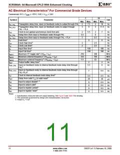
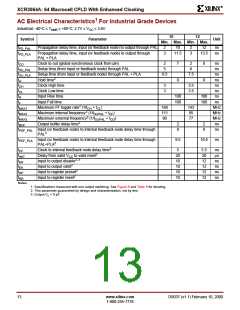
AC Electrical Characteristics1 For Industrial Grade Devices
Industrial: -40°C ≤ T
≤ +85°C; 2.7V ≤ V ≤ 3.6V
AMB
CC
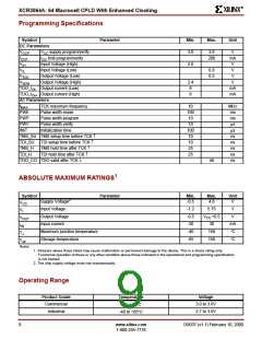
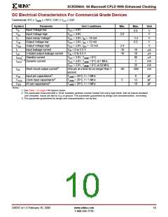
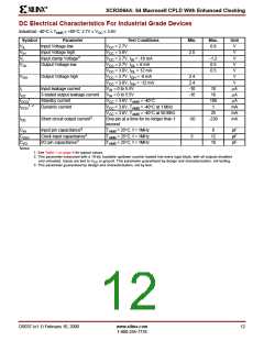
10
12
Symbol
Parameter
Unit
Min. Max. Min. Max.
t
t
Propagation delay time, input (or feedback node) to output through PAL
2
3
10
2
3
12
ns
ns
PD_PAL
PD_PLA
Propagation delay time, input (or feedback node) to output through
PAL + PLA
11.5
13.5
t
t
t
t
t
t
t
t
f
f
f
t
t
Clock to out (global synchronous clock from pin)
2
5
7
0
2
6
8
0
ns
ns
CO
Setup time (from input or feedback node) through PAL
Setup time (from input or feedback node) through PAL + PLA
SU_PAL
SU_PLA
H
6.5
7.5
ns
2
Hold time
ns
Clock High time
Clock Low time
Input Rise time
3
3
3.5
3.5
ns
CH
ns
CL
100
100
100
100
ns
R
Input Fall time
ns
F
2
Maximum FF toggle rate (1/t + t
)
166
111
90
143
95
MHz
MHz
MHz
ns
MAX1
MAX2
MAX3
BUF
PDF_PAL
CH
CL
2
Maximum internal frequency (1/t
+ t
)
SUPAL
CF
2
Maximum external frequency (1/t
+ t
)
77
SUPAL
CO
2
Output buffer delay time
2
8
2
9
Input (or feedback node) to internal feedback node delay time through
ns
2
PAL
t
Input (or feedback node) to internal feedback node delay time through
9.5
10.5
ns
PDF_PLA
2
PAL+PLA
2
t
t
t
t
t
t
Clock to internal feedback node delay time
5
5.5
20
12
12
12
12
ns
µs
ns
ns
ns
ns
CF
INIT
ER
EA
RP
RR
2
Delay from valid V to valid reset
20
10
10
10
10
CC
2, 3
Input to output disable
2
Input to output valid
2
Input to register preset
2
Input to register reset
Notes:
1. Specifications measured with one output switching. See Figure 6 and Table 6 for derating.
2. This parameter guaranteed by design and characterization, not by test.
3. Output CL = 5 pF.
13
www.xilinx.com
DS037 (v1.1) February 10, 2000
1-800-255-7778

 XILINX [ XILINX, INC ]