R
XCR3064A: 64 Macrocell CPLD With Enhanced Clocking
done. It eliminates the need for a costly, separate program-
ming step in the manufacturing process. Of course, if the
JTAG/ISP function is never required, this feature can be
turned off in the software and the device can be pro-
grammed with an industry-standard programmer, leaving
the pins available for I/O functions. Table 3 defines the ded-
icated pins used by the four mandatory JTAG signals for
each of the XCR3064A package types.
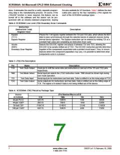
Table 2: XCR3064A Low-Level JTAG Boundary-Scan Commands
Instruction
(Instruction Code)
Register Used
Description
Bypass
(1111)
Bypass Register
Places the 1 bit bypass register between the TDI and TDO pins, which allows the BST
data to pass synchronously through the selected device to adjacent devices during
normal device operation. The Bypass instruction can be entered by holding TDI at a
constant high value and completing an Instruction-Scan cycle.
Idcode
(0001)
Boundary-Scan Register
Selects the IDCODE register and places it between TDI and TDO, allowing the
IDCODE to be serially shifted out of TDO. The IDCODE instruction permits blind inter-
rogation of the components assembled onto a printed circuit board. Thus, in circum-
stances where the component population may vary, it is possible to determine what
components exist in a product.
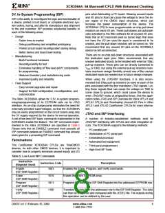
Table 3: JTAG Pin Description
Pin
Name
Description
TCK
Test Clock Output Clock pin to shift the serial data and instructions in and out of the TDI and TDO pins,
respectively.
TMS
Test Mode Select
Serial input pin selects the JTAG instruction mode. TMS should be driven high during
user mode operation.
TDI
Test Data Input
Serial input pin for instructions and test data. Data is shifted in on the rising edge of TCK.
TDO
Test Data Output
Serial output pin for instructions and test data. Data is shifted out on the falling edge of
TCK. The signal is tri-stated if data is not being shifted out of the device.
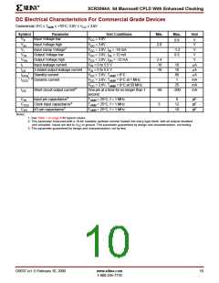
Table 4: XCR3064A JTAG Pinout by Package Type
Device
(Pin Number/Macrocell #)
XCR3064A
44-pin PLCC
44-pin VQFP
56-ball CSP
100-pin VQFP
TCK
TMS
13/B15
7/B15
TDI
TDO
38/D8
32/D8
C10/D8
73/D8
32/C15
26/C15
F10/C15
62/C15
7/A8
1/A8
G1/B15
15/B15
C1/A8
4/A8
7
www.xilinx.com
DS037 (v1.1) February 10, 2000
1-800-255-7778

 XILINX [ XILINX, INC ]